Reliability matters when you design systems that must run without failure: PhotoMOS relays give you no moving parts, which eliminates contact wear, arcing and welding that commonly cause mechanical relay failure, and they deliver longer MTBF and consistent switching over millions of cycles. You get quieter operation, faster switching, reduced maintenance and safer performance in sensitive or explosive environments, making PhotoMOS a superior choice where uptime and predictable behavior are imperative.
Types of Relays
| Type | Typical Application / Notes |
|---|---|
| Mechanical Relays | General-purpose switching up to tens of amps; common in power, automotive, and industrial systems. |
| Latching Relays | Hold state without continuous coil drive; used in memory/energy-sensitive applications. |
| Reed Relays | Fast, low-contact-force switching for low-voltage signals; good for test and instrumentation. |
| Solid-State Relays (SSRs) | Includes MOSFET- and TRIAC-based SSRs for silent, contactless switching of DC/AC loads. |
| PhotoMOS Relays | Opto‑driven MOSFET switches offering long life, high isolation and low leakage for precision and safety-critical designs. |
- Mechanical Relays: moving contacts, contact bounce (~1-5 ms), lifetimes typically in the 10^4-10^7 cycle range under rated load.
- Reed Relays: glass-encapsulated contacts, low capacitance and fast switching for low-power signals.
- PhotoMOS Relays: optically isolated MOSFETs with lifetimes often exceeding 10^8 cycles and isolation ratings up to several kVrms depending on part.
- SSRs: silent switching, immunity to contact wear, but watch on-resistance and leakage for low-level signals.
- Latching Relays: minimize holding power; suitable when you need state retention through power cycles.
Mechanical Relays
You will see Mechanical Relays specified by coil voltage (commonly 5-24 VDC), contact ratings (from a few hundred milliamps to 30 A+), and electrical life quoted as a range-often 10^4-10^7 operations at rated load; in lighter signal use that life can be much higher. Switching times are typically in the 5-20 ms window, with contact bounce on the order of 1-5 ms that forces you to add debounce or suppression if you care about clean transitions.
When you switch inductive or high-inrush loads with a mechanical relay you must mitigate arcing and contact welding using snubbers, TVS diodes, or RC networks; contact materials such as AgSnO₂ and the contact gap geometry determine wear rate. In field cases-industrial contactors for motors, for example-contacts can weld after only thousands of cycles under severe arcing conditions, so your choice of relay and protective circuitry directly affects maintenance intervals and safety.
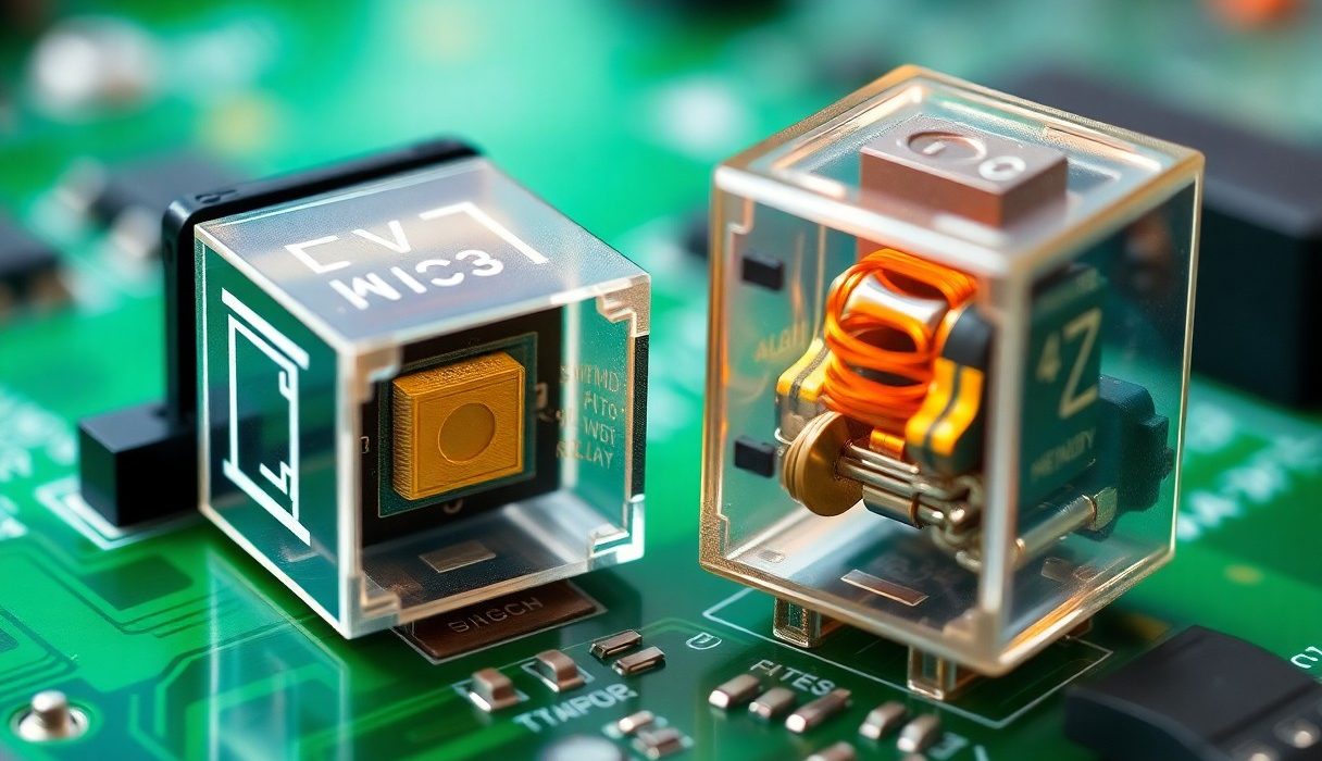
PhotoMOS Relays
You will find PhotoMOS Relays implement an LED driving an optically coupled MOSFET pair (or array), eliminating moving parts and virtually eliminating arcing, contact bounce, and mechanical wear. Typical parts offer switching from microseconds to low milliseconds, isolation ratings up to ~5 kVrms on some families, and lifetimes commonly specified as >10^8 cycles; leakage currents range from nanoamps to microamps depending on model, so they suit precision analog or safety-isolated digital paths.
Expect trade-offs: on-resistance (RDS(on)) varies widely-some low-current parts are tens of ohms while power PhotoMOS devices drop below an ohm-and continuous current capability is usually limited to a few amps at most, so your thermal design and voltage drop matter. Manufacturers publish thermal resistance and power‑dissipation curves you must consult; in practice, PhotoMOS relays excel where longevity, silence, and isolation outweigh the need to carry very high continuous currents.
In many medical and instrumentation case studies you’ll see PhotoMOS Relays used for channel isolation and repeated-test applications precisely because they remove contact maintenance and produce predictable drift over millions of operations while maintaining signal integrity for low‑level measurements.
Thou must weigh lifecycle, on-resistance, and the presence of arcing against your application’s current, voltage, and isolation requirements when selecting between PhotoMOS Relays and Mechanical Relays.
Factors Influencing Reliability
Several variables determine long-term performance when you compare PhotoMOS relays and mechanical relays. Key elements include switching mechanism, thermal management, electrical load profile (steady DC vs. high inrush AC), and the operating environment such as temperature, humidity, and vibration. For example, a mechanical relay specified for 106-107 cycles under rated load will degrade far faster than a typical PhotoMOS device that manufacturers rate for 108-109 operations in low-stress switching, especially when you keep junction temperatures low.
- Operating principles (contact vs. solid-state switching)
- Electrical stress (inrush current, switching frequency, load type)
- Thermal management (Tj, ambient, derating)
- Environmental conditions (humidity, altitude, vibration, corrosive atmospheres)
- Manufacturing quality and part-to-part variability
Operating Principles
Because you’re dealing with fundamentally different mechanisms, the failure modes diverge: mechanical relays rely on metal contacts that open and close, so you get wear from contact erosion, pitting, and contact bounce; those effects intensify under high inrush (motor starts, lamps) where contact temperatures spike and contact welding can occur within milliseconds. In contrast, PhotoMOS relays use light-driven MOSFETs or optically coupled semiconductor switches, which eliminate arcing and contact wear but introduce semiconductor-specific issues such as Rds(on) drift, hot‑carrier degradation, and thermal runaway if you exceed datasheet derating curves.
You should assess lifetime differently: mechanical devices often fail through discrete, sudden events (stuck contacts, welded contacts), while PhotoMOS failures tend to be gradual (increasing on-resistance, leakage rise). Practical design examples show mechanical relay maintenance cycles shortening from years to months when switching heavy inductive loads daily, whereas a properly derated PhotoMOS can sustain millions of cycles without a single macro failure, provided you control junction temperature and stay within the specified continuous current and voltage limits.
Environmental Conditions
Environmental stressors change the balance of advantages: you’ll find mechanical relays particularly vulnerable to corrosive atmospheres and high humidity, where contact oxidation increases contact resistance and intermittent operation becomes common. PhotoMOS devices avoid exposed contacts, so no arcing and no contact corrosion means you can deploy them in damp or salty environments more confidently, but you must still manage encapsulation ingress protection (IP rating) and board-level conformal coatings to prevent condensation-related leakage paths.
Temperature extremes affect both types but in different ways. For PhotoMOS, junction temperature is the limiting factor – many parts specify a maximum Tj around 125°C and require derating above ~85°C ambient; exceeding that accelerates lifetime-limiting mechanisms and increases leakage current. Mechanical relays often tolerate higher external case temperatures for short periods, yet repeated thermal cycling leads to spring fatigue and contact deformation, and vibration at resonant frequencies can cause chattering that increases wear.
Vibration and shock present another contrast: if your application (e.g., industrial machinery or automotive) exposes components to continuous vibration, you must account for contact bounce and set solder and mechanical mounting practices accordingly for mechanical relays; for PhotoMOS, focus on solder joint reliability and package board adhesion, since the internal semiconductor has no moving parts to fatigue.
After you weigh thermal derating curves, inrush profiles, humidity susceptibility, and vibration tolerance against your system requirements, you can select the relay type and protective measures that maximize your overall reliability.
Pros and Cons of PhotoMOS Relays
| Pros | Cons |
|---|---|
| Contactless switching eliminates bounce and mechanical wear | Higher ON resistance than ideal mechanical contacts – causes voltage drop and heat |
| Very long cycle life – vendors quote lifetimes in the range of millions to billions of operations | Off-state leakage (from nanoamps to microamps) can spoil high‑impedance sensor paths |
| Fast, repeatable switching (typical response from tens of microseconds to a few milliseconds depending on model) | Continuous current ratings commonly limited to a few amps unless you pick power variants |
| High galvanic isolation and good EMI performance for many control/telecom applications | Thermal derating is significant – you must manage power dissipation and PCB heat sinking |
| No arcing, so safer in frequent switching and dust-prone environments | Not ideal for switching large inductive loads without snubbers or special protection |
| Small package and easy drive from logic-level voltages simplifies board design | Higher unit cost for high-voltage or high-current variants compared with simple mechanical relays |
| Predictable electrical characteristics – good for precision instrumentation and automated test | Some devices require specific polarity or bidirectional arrangements for AC switching |
| Lower audible noise and no moving parts, useful in consumer and medical devices | Limited surge and inrush tolerance compared with heavy-duty mechanical contacts |
Advantages
You gain high reliability from the PhotoMOS architecture because there are no physical contacts to erode or weld; manufacturers typically rate these devices for millions to billions of cycles, which translates into decades of service in low‑duty applications. When you need repeatable timing or zero contact bounce for digital gating, PhotoMOS relays give deterministic switching in the range of tens of microseconds to a few milliseconds depending on the part – this is why system designers use them in telecom line cards and automated test equipment where cycle count and timing consistency matter.
Performance-wise, you can pick parts that trade off on‑resistance, leakage and voltage rating to match your application: power variants deliver sub‑ohm RON for currents of 1-2 A or more, while small‑signal types offer ultra‑low capacitance and excellent isolation for high-speed analog paths. In practice, that means you can replace multiple mechanical relays with a compact PhotoMOS array to save board space and improve MTBF without sacrificing signal integrity in many control and measurement systems.
Disadvantages
You will encounter limitations that change how you design protection and thermal budgets. PhotoMOS devices have a measurable ON resistance that causes voltage drop and dissipates power – if you pass continuous currents in the ampere range you must calculate I²R losses and apply thermal derating or choose a power-rated relay. Also bear in mind their off‑state leakage (typically nA-µA): when you switch high‑impedance sensor inputs or sample-and-hold nodes, that tiny leakage can create measurement errors unless you add buffering or pull‑downs.
Operationally, PhotoMOS relays handle inductive loads and large inrush poorly compared with heavy mechanical contacts: you should add snubbers, TVS diodes or current-limiting to protect the MOSFETs. In addition, many single-ended PhotoMOS parts are optimized for DC or unidirectional switching – for AC mains or bidirectional signals you often need specialized bidirectional packages or two MOSFETs in series, which increases cost and complexity. Exceeding ratings can cause overheating and device failure, so fuse and thermal monitoring are good practice.
Tips for Choosing the Right Relay
Match the relay to the load
You should size the relay first to the steady-state and inrush currents of your load: PhotoMOS relay parts often handle continuous currents from 0.2 A to several amps with ON-resistance ranging from tens of milliohms to a few ohms, while mechanical relay contacts commonly support higher peak currents but degrade after roughly 10^5-10^7 operations. For fast digital switching or PWM you’ll value switching speed–PhotoMOS relays typically switch in microseconds-to-milliseconds versus tens of milliseconds for mechanical types. Also factor in contact arcing risk on AC inductive loads: if you switch >1 A AC inductive loads frequently, use snubbers, RC networks, or choose a relay rated for inductive duty to avoid contact arcing and premature failure.
- Derate continuous current by 20-30% for ambient >50 °C; thermal limits directly affect MTTF.
- Pick isolation and safety ratings (creepage and isolation voltage) that exceed your system peak by 25-50% for margin.
- Prefer PhotoMOS relay for >10^6 daily cycles or when silent operation and no contact wear are required.
- Choose mechanical relay for very high surge currents or when galvanic separation for power lines is mandatory.
- Verify package (SMD vs through-hole), mounting vibration spec, and any required certifications (UL/IEC) for your application.
Consider environment, reliability and lifecycle cost
When you evaluate long-term reliability, compare datasheet MTTF and contact life: many PhotoMOS relays quote >10^8-10^9 switching cycles and negligible contact wear, so in high-cycle applications they typically cut maintenance and field-repair costs substantially. In harsh environments check for humidity, salt fog, and vibration ratings-mechanical contacts can fail from contact pitting, while solid-state devices can be limited by package thermal resistance and absolute maximum voltages. Balance total cost by modeling expected replacement intervals and downtime impact; for example, if your system performs 10,000 switches per day, a device rated for 10^9 cycles provides multi-year service without contact wear, whereas a 10^6-cycle mechanical relay would need replacement in roughly 100 days under the same duty.
Any choice you make should weight load type, environmental stresses, safety margins for isolation voltage, and realistic lifecycle costs so you select the relay that minimizes risk and long‑term service effort.
Step-by-Step Installation Guide
Preparing the board and components
Start by verifying the PhotoMOS part number against the load: check the maximum load current (example: up to 2.0 A for high-current types), the maximum voltage (typical ranges: 60-150 V), and the isolation rating (often 3750 Vrms). When you calculate the LED drive resistor, use the formula R = (Vdrive − Vf) / If; for example, with a 5 V MCU output, Vf ≈ 1.2 V and If = 10 mA, choose R ≈ 380 Ω. Protect the input with a series resistor sized for your microcontroller and include a flyback path only if switching inductive loads-PhotoMOS devices will still need protection against transients above their rated surge current. Keep ESD-sensitive handling practices in place and place the relays away from hot components; if you anticipate continuous currents >0.5 A, plan for board copper heatsinking or derate the device to <70% of its continuous rating at ambient temperatures above 40 °C.
Mounting, soldering and bench testing
Position the device using the manufacturer’s footprint and orient the pins so the marking aligns with your schematic; incorrect polarity on input LEDs or mis-wiring the outputs can permanently damage the relay. For reflow, follow a typical Pb-free profile with peak ≈ 245 °C for ≤30 s and avoid prolonged exposure to high temperatures; for hand-soldering, limit contact time per pin to the manufacturer’s recommendation. After assembly, run a functional test: drive the LED at the intended current (for example 10-20 mA), measure on-resistance (Rds_on) and off-state leakage, and perform an endurance run of at least 10,000 cycles at the target load-lab tests commonly show PhotoMOS lifetimes >10^8 cycles versus mechanical contacts often below 10^6 in similar duty. If you encounter excessive heating (>10-15 °C rise at rated current) or R_on drift, reduce duty, add copper area, or select a higher-current PhotoMOS variant.
Installation Steps
| Step 1 | Verify ratings: load current, voltage, isolation (e.g., 2 A, 60 V, 3750 Vrms). Check datasheet for surge and R_on values. |
| Step 2 | Calculate input resistor: R = (Vdrive − Vf)/If. Example: 5 V drive, Vf ≈ 1.2 V, If = 10 mA → R ≈ 380 Ω. |
| Step 3 | PCB footprint & orientation: use manufacturer footprint, leave thermal copper under package for >0.5 A continuous use. |
| Step 4 | Soldering profile: Pb-free reflow peak ≈ 245 °C ≤30 s; avoid prolonged heat exposure to prevent internal damage. |
| Step 5 | Protection: add surge/snubber if switching inductive loads; prevent currents above rated surge or permanent failure may occur. |
| Step 6 | Test: functional check at nominal current, measure R_on and leakage, run endurance cycles (lab goal ≥10,000; many designs target 10^7-10^8). |
Maintenance Best Practices
Inspection and Monitoring
Inspect assemblies visually every 6-12 months in normal environments and monthly in harsh sites (high humidity, dust, vibration). Use a thermal camera and a simple leakage test rig during scheduled checks: many PhotoMOS parts list off‑state leakage in the range of 1 μA to 100 μA and on‑resistance spanning from under an ohm for low‑RDS(on) types to several ohms for general‑purpose devices, so log those values and flag any >10× deviation. Field reports show that after switching from mechanical relays to PhotoMOS in conveyor control panels, teams reduced relay‑related interventions from multiple per month to annual electrical verifications only; in those cases the most telling early signs were rising leakage and localized hot spots on the PCB.
Preventive Measures and Replacement Criteria
Derate and protect: operate PhotoMOS devices at no more than about 70% of their rated continuous current, keep ambient below ~60 °C where possible, and fit TVS diodes or RC snubbers to absorb transients so you don’t exceed surge or dV/dt limits. Replace a unit if you observe sustained leakage above the datasheet limit by an order of magnitude, an increase in on‑resistance greater than ~20%, visible solder cracks or delamination, or repeated thermal excursions; these are the failure modes that predict end‑of‑life for solid‑state relays. While mechanical relays often demand contact cleaning every 6-12 months in dirty environments, PhotoMOS removes contact wear and gives you significantly reduced maintenance interventions-your maintenance focus shifts to thermal control, surge protection, and solder‑joint integrity.
To wrap up
Drawing together the technical advantages, you see that PhotoMOS relays deliver higher reliability because they remove moving parts that fail from wear, eliminate contact bounce and arcing, and resist shock, vibration, and contamination that degrade mechanical relays. By providing predictable, repeatable switching with long cycle life and low maintenance, they reduce failure rates in applications where consistent operation matters most to your system uptime.
You should still design for the device’s limitations – manage thermal dissipation, voltage and current ratings, and derating – but when specified and cooled properly, PhotoMOS relays offer more robust, deterministic performance and lower lifecycle risk than mechanical alternatives for many demanding environments.