Most systems suffer measurable performance loss from high contact resistance, so you should measure and monitor interface resistance, clean mating surfaces, ensure correct contact pressure, and use appropriate platings or lubricants to reduce corrosion. By taking these steps you prevent excess heat and failure risk and achieve higher efficiency and longer component life, while routine testing and torque control deliver the most reliable electrical connections for your system.
Understanding Contact Resistance
Definition and Importance
When you inspect joints and connectors, contact resistance is the localized opposition to current where two conductive surfaces meet; it directly causes voltage drop and heat generation. For example, a contact that rises to 50 mΩ at 5 A produces a 0.25 V drop and dissipates 1.25 W, which can shift thermal balance, accelerate material degradation, and upset sensitive measurements in your system.
Because your system performance depends on predictable rails and low losses, even milliohm-level changes matter: in a 12 V, 10 A rail an extra 10 mΩ adds ~1 W of loss and reduces delivered voltage by 0.1 V. Field data show oxidized aluminum interfaces can climb from under 1 mΩ to over 100 mΩ within months in corrosive environments, greatly increasing failure and thermal-runaway risk.
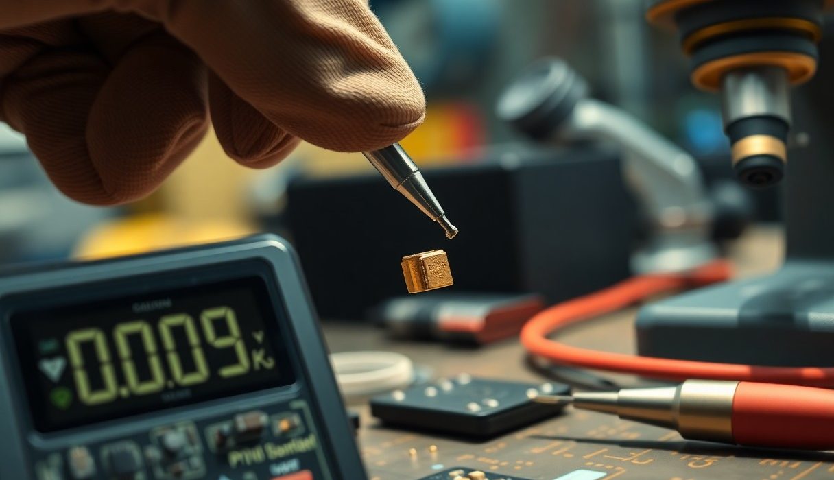
- Measurement: use four-wire Kelvin techniques to isolate true contact resistance.
- Impact: small increases cause outsized effects on precision sensors and high-current distribution.
- Thou prioritize surface cleanliness and consistent contact force to limit resistance growth.
Types of Contact Resistance
You need to distinguish two dominant mechanisms: constriction resistance, where current is forced through microscopic asperities (a-spots) and concentrates, and film resistance, caused by non-conductive layers like oxides or contamination. Constriction typically yields milliohm-level contributions per contact spot, while films can add orders of magnitude more; for instance, a thin oxide layer on aluminum often pushes resistance into the tens to hundreds of milliohms range.
Material and mechanical factors govern which type dominates: copper joints with proper mating and torque show very low constriction losses (<1 mΩ for well-designed bolted joints), whereas aluminum contacts without plating quickly develop film resistance. You should also account for dynamic effects like fretting corrosion, which can convert low-resistance contacts into high-resistance failures over thousands of cycles.
Testing and mitigation are practical: use four-wire micro-ohm meters for repeatable measurements, specify gold plating or controlled torque to keep film resistance <1-10 mΩ in many connector designs, and apply contact lubricants or redesign contact geometry for high-current paths; field case studies show replacing unplated aluminum pins with gold-plated copper reduced contact resistance from ~120 mΩ to <5 mΩ and cut connector heating by over 90% during 20 A operation.
- Constriction: sensitive to surface roughness and contact pressure.
- Film: dominated by oxide chemistry and contamination; plating mitigates it.
- Thou verify resistance under expected temperature and vibration profiles during qualification.
| Category | Notes / Typical values |
| Constriction resistance | Microscopic a-spots produce mΩ-level resistance; improves with higher contact force. |
| Film resistance | Oxides/contaminants can exceed 100 mΩ; mitigated by plating and cleaning. |
| Material factors | Aluminum forms insulating oxides; copper remains conductive and is preferred for low resistance. |
| Measurement & mitigation | Use four-wire (Kelvin) measurement, specify torque, plating, and consider soldered or welded joints for sub-mΩ performance. |
Factors Influencing Contact Resistance
Many interacting variables determine the effective contact resistance you see in service; you need to treat them as a system rather than isolated causes. Mechanical factors such as contact force and real contact area interact with metallurgical attributes like material properties, plating chemistry and native oxidation, while environmental drivers-temperature, humidity and contamination-can rapidly change resistance over hours or years. Quantitatively, a thin oxide layer of just 1-50 nm can increase contact resistance by one to several orders of magnitude, and reducing surface roughness from Ra 1.0 µm to Ra 0.1 µm commonly cuts resistance by tens of percent in connector tests.
- Material properties (bulk conductivity, hardness, work-hardening)
- Surface finish (Ra, Rz, micro-asperities)
- Coatings and platings (gold, silver, nickel barriers)
- Contact force and compression behavior (N per contact, MPa pressure)
- Oxidation/corrosion and contamination (organic films, salts)
- Temperature and thermal cycling effects
This requires you to prioritize measurements and mitigations that match your failure modes and operating environment.
Material Properties
You must consider intrinsic conductivity and mechanical behavior when selecting contact metals: copper (≈ 1.68×10⁻⁸ Ω·m) and silver (≈ 1.59×10⁻⁸ Ω·m) give the lowest bulk resistivity, while gold (≈ 2.44×10⁻⁸ Ω·m) offers superior corrosion resistance at slightly higher resistivity. Hardness and yield strength determine how much asperity flattening occurs under load-softer metals will increase real contact area at lower forces, reducing resistance, but may wear faster in high-cycling contacts.
In practice you choose platings as trade-offs: a thin gold plating flash (30-100 nm) stabilizes contact resistance for low-cycle applications, while a thicker gold layer (>0.5 µm) or gold over a nickel barrier (2-5 µm) is used for harsh environments. Silver plating yields the lowest immediate contact resistance but is susceptible to tarnish (sulfidation) unless protected; specifying plating thickness and barrier layers reduces long-term variability.
Surface Finish and Preparation
Surface topography controls the proportion of nominal area that actually conducts current: microscopic asperities concentrate current and heat, so you aim for lower Ra values to increase uniform contact. Typical board-to-board or connector performance improves when you move from machined finishes (~Ra 0.8-1.6 µm) to polished finishes (Ra 0.05-0.2 µm), and manufacturing examples show resistance drops of 20-50% after controlled polishing or burnishing.
Cleaning and handling are equally important: fingerprints and machining oils can raise contact resistance by factors of 2-10, while native oxides (aluminum 2-5 nm, copper 5-20 nm) form within minutes and must be controlled by surface treatment, flux selection or plasma/chemical cleaning. You should specify assembly controls-cleaning solvent, wipe protocol, and humidity limits-to prevent early-life resistance growth.
More detailed metrics help you control outcomes: use a Kelvin four-wire fixture to measure low-ohm contacts accurately, inspect finish with profilometry to target an Ra window, and validate cleaning by contact-resistance frequency testing; documented case studies show burnishing a 0.6 mm gold-plated contact under 1.0 N spring force can reduce resistance from 40 mΩ to 25 mΩ per contact, improving thermal margin in high-current designs.
Tips for Reducing Contact Resistance
Start by mapping the highest-loss interfaces in your system and prioritize changes where a small drop in contact resistance yields large system gains – for example, a 10 mΩ reduction at a power bus carrying 50 A saves 5 W of dissipated power. Apply combinations of design and process measures: increase nominal contact area where mechanical constraints allow, raise normal contact force within wear and actuation limits, and replace oxidizable finishes on high-current nodes with more stable coatings. Use quantitative acceptance criteria (target contact resistance values and maximum allowable drift over time) and verify with repeated milli-ohm measurements under representative environmental and mechanical cycling.
Implement these practical steps in parallel:
- Material selection: choose higher-conductivity alloys or plating stacks.
- Surface treatments: specify plating thickness, underlayers, and post-plating cleaning.
- Contact geometry: increase width, add redundant pads, or use multiple contact points.
- Mechanical design: increase spring force or incorporate wiping action to disrupt films.
- Maintenance: establish cleaning intervals and use approved conductive lubricants sparingly.
Recognizing that effective reductions usually come from a combination of these tactics, plan test matrices that change only one variable at a time so you can quantify each measure’s impact.
Optimal Material Selection
You should favor base metals and alloys with high bulk conductivity and suitable mechanical properties: copper (≈5.96×10^7 S/m) and silver (≈6.30×10^7 S/m) outperform common brasses (≈1.6×10^7 S/m) when low resistance is the objective. For spring contacts where resilience matters, beryllium copper or phosphor bronze provide better elastic return than pure copper, while a copper alloy base plated with a thin noble metal balances conductivity, wear resistance, and manufacturability.
When comparing finishes, quantify lifetime and environment: bench studies commonly report a 20-60% reduction in steady-state contact resistance when switching from tin-plated brass to gold-plated copper on low-force signal contacts, and gold or silver platings reduce oxidation-related drift in humid/sulfurous atmospheres. Balance cost – gold is expensive above ~0.5 µm thickness – against required performance and expected cycles; specify minimum plating thickness and test per relevant contact cycling standards to validate your choice.
Effective Surface Treatments
You can dramatically reduce initial and long-term contact resistance by controlling the finish stack and post-process handling: employ a corrosion-resistant noble surface (gold or silver) over a diffusion barrier such as nickel, and specify plating thickness appropriate to the application – for example, gold plating in the range of 0.05-2 µm (50-2000 nm) for connectors, with thicker deposits (≥1 µm) where abrasive wear or frequent mating is expected. Prevent underplating failures by ensuring proper adhesion and by avoiding exposed tin on power contacts because of tin whiskers and fretting corrosion risks.
Prepare surfaces with controlled mechanical and chemical cleaning: target a final surface roughness that matches contact type (Ra ~0.1-0.4 µm for stable metal-to-metal contact in high-reliability connectors), use plasma or ultrasonic cleaning to remove oils and particulates before plating, and apply anti-corrosion passivation where appropriate. Include validation such as Kelvin four-terminal resistance measurements, thermal cycling, and fretting tests to confirm that the chosen surface treatments preserve low resistance over the expected service life.
For assemblies exposed to vibration or contaminants, consider conductive lubricants (silver- or graphite-filled) only after testing for added series resistance, EMI effects, and long-term migration; in many field cases a thin controlled lubricant layer reduces micro-welding and fretting growth, but improper selection can increase noise in low-level signals, so you should specify lubricant type and application thickness in your maintenance procedures.
Step-by-Step Guide to Improving Performance
Action Checklist
| Step | Details & Examples |
|---|---|
| Map & Prioritize | Use load profiles and thermal scans to identify top 10% loss points; target the top 3 interfaces first for highest ROI. |
| Measure Baseline | Perform four-wire (Kelvin) micro-ohm measurements and loaded voltage-drop tests; capture temperature rise with an IR camera at rated current. |
| Analyze Causes | Inspect plating, contact area, mechanical pressure and contamination; compare against spec (torque, plating thickness, contact gap). |
| Implement Fix | Apply re‑torque to spec, replace corroded contacts, increase contact area, or convert to welded/larger-terminals where applicable. |
| Verify & Monitor | Re-measure under load, run a 1-4 hour soak test, and schedule periodic thermal checks and logged resistance readings. |
Assessment of Existing Connections
You should start by quantifying each interface under real operating conditions: use a four‑wire micro‑ohmmeter to measure contact resistance and perform a loaded voltage-drop test at a representative current (for example, 100-300 A for power racks or 5-20 A for signal harnesses). Combine those readings with an infrared thermal scan-hotspots that exceed ambient by >15-20 °C at rated current typically indicate contact resistance an order of magnitude higher than design intent. Record ambient, current, measured milliohms, and temperature for every connection so you can rank interventions by energy loss and safety risk.
Next, inspect mechanical and surface factors that explain elevated readings: check plating wear, visible oxidation, contact geometry (edge vs full-face), and retention hardware. Use a calibrated torque wrench and force gauge to verify contact pressure against manufacturer specs; deviations of ±15% from specified torque often correlate with measurable resistance increases. For example, a lug that measured 5 mΩ under 200 A produced a 1 V drop and 200 W loss-reduced to 1 mΩ after correction, the same joint dropped to 0.2 V and 40 W, showing how quantified assessment guides priority selection.
Implementation of Solutions
When you act, follow a defined sequence: de‑energize and lock out the circuit, document pre‑work readings, then apply the chosen fix-cleaning with isopropyl alcohol and non‑abrasive pads for light contamination, abrasive resurfacing or replacement for pitted/oxidized contacts, and re‑torquing to exact spec for fastened joints. For high‑current busbars and lugs consider increasing contact area (parallel conductors or larger terminals) or switching to welded/tinned terminations; similarly, use spring‑loaded contacts or compliant connectors in applications with vibration. Avoid mixing incompatible platings and metals; if you must join aluminum-to-copper, use an approved anti‑oxidant compound and explosion‑rated connectors to prevent galvanic degradation.
Verify results under load after implementation: re-measure contact resistance with the four‑wire method, run a soak at rated current while monitoring temperature, and log voltage drop and thermal images. You should expect proportional reductions in I²R losses-for instance, lowering a joint from 5 mΩ to 1 mΩ at 200 A cuts thermal loss from 200 W to 40 W (an 80% reduction), which both improves efficiency and lowers hotspot risk. Maintain a change log with before/after values and schedule follow‑up inspections at intervals determined by operating duty (e.g., 3 months for high‑duty systems, 12 months for stable installations).
Pros and Cons of Methods
| Pros | Cons |
|---|---|
| Lower conduction losses – halving contact resistance halves I²R losses (e.g., at 100 A, 1 mΩ → 10 W dissipation). | Higher material cost – noble-metal platings or specialty alloys can increase part cost by roughly 5-25% depending on volume and spec. |
| Reduced thermal hotspots and improved safety – measured temperature drops of 10-30°C reported in EV module assemblies after improved joining. | Increased process complexity – laser welding, ultrasonic welding or controlled crimping require capital equipment and trained operators. |
| Better signal integrity for low-voltage/high-speed lines – lower contact resistance reduces insertion loss and jitter in sensitive circuits. | Tighter mechanical tolerances – many high-performance contacts need micron-level alignment or controlled contact force to maintain low resistance. |
| Longer component life and lower maintenance frequency – fewer re-torques and less thermal cycling stress on joints. | Coating wear and fretting – without proper surface treatment or locking, contact resistance can rise over months/years. |
| Enables higher current density and smaller conductors – you can downsize busbars or traces to save weight and volume. | Galvanic corrosion risk – mixing dissimilar metals for low resistance can accelerate corrosion unless mitigated. |
| Predictable thermal profile simplifies cooling design – lower and more uniform heat generation eases heatsink sizing. | Greater inspection and QC burden – you may need four-wire measurements, microscopy, and batch qualification, adding time and cost. |
| System-level energy savings at scale – data centers and traction systems see measurable kWh and fuel/energy reductions. | Longer validation cycles – qualifying new contact methods can add weeks to months to product development timelines. |
| Improved reliability in safety-critical applications – fewer thermal failures and better redundancy behavior. | Repairability challenges – laser- or welded joints are harder to rework in the field compared with simple mechanical fasteners. |
Advantages of Reduced Contact Resistance
You gain immediate thermal and efficiency benefits: halving a joint’s resistance directly halves its I²R losses, so at typical powertrain currents (hundreds of amps) that translates to tens or hundreds of watts less heat per joint. In practice, manufacturers report system-level efficiency improvements of 1-3% in high-current assemblies after switching from crimped to welded or plated contacts, and you lower the probability of localized overheating that leads to degraded insulation or smoke.
Operationally, you also reduce maintenance overhead and improve lifecycle performance. For example, fleets that implemented controlled-welded connections saw a drop in connector-related failures and fewer torque-check maintenance cycles; likewise, in telecom racks, lowering contact resistance by a few milliohms across busbars reduced cooling load and improved uptime. When you design with lower contact resistance, cooling systems can be smaller and your parts can be lighter without sacrificing safety.
Potential Drawbacks
Lowering contact resistance can introduce cost and manufacturability trade-offs: switching to silver or gold platings, or to laser-welded joints, raises component and process costs and often requires new fixtures, training, and inline inspection. You should expect qualification campaigns to take additional time-typically weeks to months-and budget for higher initial capital expenditure and increased per-unit cost on low-volume runs.
Long-term reliability risks can also arise if you don’t address wear mechanisms and material compatibility. For instance, coatings that initially give sub-milliohm contacts may degrade via fretting or galvanic action, causing resistance to climb; environmental exposure (salt spray, humidity) can accelerate that. In critical systems, a rising contact resistance can concentrate heat and create a failure mode that is both gradual and hard to detect without periodic four-wire checks.
Mitigation requires disciplined design and process controls: you should specify compatible base metals, consider protective coatings or conductive lubricants while weighing their assembly implications, enforce torque/force tolerances (e.g., ±10%) during assembly, and implement targeted in-line resistance measurements and environmental testing to catch early degradation before it affects system safety or performance.
Monitoring and Maintenance
Regular Performance Checks
Schedule routine inspections that combine visual, mechanical, and electrical checks: perform visual inspections monthly, torque audits quarterly using a calibrated torque wrench set to manufacturer specs, and 4‑wire (Kelvin) contact resistance measurements at rated current every 3-6 months. Use thermal imaging during load to catch developing hotspots; treat any local temperature rise of more than 20°C above ambient or absolute joint temperatures exceeding 60°C as an immediate fault condition requiring corrective action.
Log every measurement into your CMMS or a simple trending spreadsheet so you can detect slow degradation-set alarms for slope changes rather than single outliers. For example, one discrete manufacturing site cut unplanned downtime by 35% after instituting weekly thermography and quarterly resistance trending; hotspots that once peaked at 45°C were reduced to under 25°C within two maintenance cycles. Where possible, deploy remote temperature sensors or current monitors to give you continuous visibility and trigger inspections when thresholds are crossed.
Long-term Solutions
Upgrade materials and fastening methods to remove the root causes of contact resistance: replace tin‑plated connectors with silver or gold plating for low-contact-resistance signal points, use larger cross‑section busbars or parallel conductors to reduce current density, and where feasible convert bolted joints to welded or brazed joints to eliminate mechanical relaxation. In many high-current installations, increasing contact area or switching to silver-plated copper can cut contact resistance by up to 50%, dramatically reducing I²R losses and hotspot formation.
Rethink system architecture to make contact resistance a design parameter rather than an afterthought: specify conductor sizing so that current density stays below targeted limits (for example, aim for under 5 A/mm² on critical bus runs), add redundant parallel paths to halve resistance, and select IP‑rated connectors or conformal coatings in corrosive environments to slow oxidation rates. One data center that doubled busbar area and added parallel feeds reduced voltage drop by ~40% and eliminated several thermal alarm events that previously triggered emergency maintenance.
Quantify the ROI before committing: calculate energy savings using I²R-reducing a joint resistance from 10 mΩ to 2 mΩ at 500 A, for instance, cuts dissipated power by 2,000 W (500²×0.008), which quickly offsets upgrade costs in continuous‑load systems. Pilot the changes on a single feed, monitor pre/post thermal and resistance baselines, and scale the upgrades where you validate the expected payback and reliability gains.
Summing up
Hence you can materially improve system performance by systematically locating and reducing contact resistance: employ diagnostic methods such as four‑wire resistance measurements and thermal imaging, prioritize cleaning, corrosion removal, and appropriate plating, and enforce correct assembly practices like controlled torque, reliable soldering, and optimized spring or wipe contact designs so your connections carry current with minimal loss and heat.
By implementing these measures and integrating simple monitoring and preventive maintenance into your procedures, you will extend component life, increase energy efficiency, reduce downtime, and achieve more predictable system behavior, yielding lower operating costs and greater reliability across your installations.