There’s a need to understand how PhotoMOS devices use optically coupled LEDs and MOSFETs to provide galvanic isolation up to high voltages, so you can design systems that maintain signal integrity while protecting your users and equipment from hazardous ground faults and high-voltage transients. This guide explains how isolation is achieved, the trade-offs in leakage, on-resistance, and switching speed, and how you can select and apply PhotoMOS relays to maximize reliability and safety.
Understanding Optical Isolation
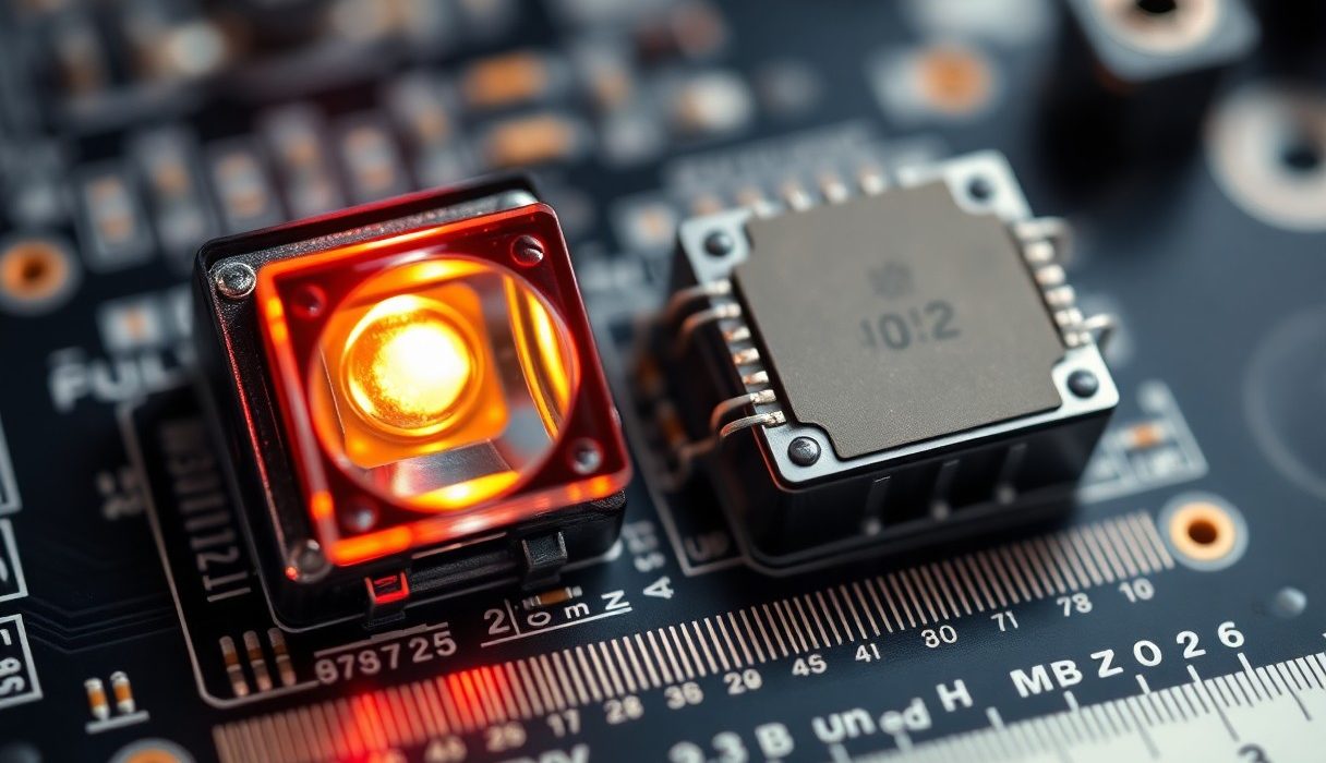
In PhotoMOS devices, optical isolation means the signal path between your input and output is broken by a light-based barrier: an LED drives a photodetector that, in turn, actuates a MOSFET output without any direct conductive path. That barrier is implemented with a physical gap and insulating materials so the device can withstand high common-mode stress; many PhotoMOS parts are specified for isolation withstands in the low kilovolt range (commonly on the order of 2-4 kVrms) and can handle load voltages of several hundred volts in practical circuits.
Because the transfer is optical rather than galvanic, you get benefits in system safety and noise immunity, but you must also manage side effects: off‑state leakage and output capacitance can create ghost voltages on high‑impedance nodes, and the ON resistance of the MOSFET (which varies by family from sub‑ohm to tens of ohms) sets your power dissipation and thermal limits. When you design PCBs with PhotoMOS parts, pay attention to creepage/clearance, thermal derating curves, and the device’s input LED drive requirements so isolation integrity and reliability are preserved.
What is Optical Isolation?
Optical isolation is the method of transmitting control information via photons rather than electrons across a barrier, so your control circuitry is electrically separated from the load. In PhotoMOS technology specifically, an LED input typically requires a modest drive (often in the range of 1-20 mA depending on the part) to generate light that activates an integrated photodetector and MOSFET driver; the result is a solid‑state switch that operates without metal contacts and provides a defined breakdown and isolation rating between input and output.
The practical implication for you is that switching characteristics are deterministic and fast compared with mechanical relays: PhotoMOS devices commonly switch in the tens to hundreds of microseconds range, offering higher cycle life and less contact‑bounce noise. At the same time, you must account for device parameters such as input‑to‑output transfer function (LED current vs. RON), output capacitance (which affects AC leakage and transient behavior), and RON variability with temperature when sizing for real‑world loads.
Importance in PhotoMOS Technology
Optical isolation is the feature that enables PhotoMOS relays to be used in safety‑sensitive and precision applications: you can place them between high‑voltage, noisy, or patient‑connected circuits and your low‑voltage electronics to prevent ground loops and protect users and instruments. For example, in measurement front‑ends and medical monitoring, engineers commonly choose PhotoMOS devices because their no‑contact operation delivers millions to billions of cycles and predictable isolation ratings that help meet regulatory safety margins.
That said, you should weigh tradeoffs: PhotoMOS parts typically have limited continuous current capability (from a few hundred milliamps up to a few amps depending on the family) and may not tolerate large surge currents without additional protection. Also, off‑state leakage currents and output capacitance can interfere with high‑impedance sensing circuits, so design mitigations such as bleeder resistors or snubbers are often necessary.
When applying this in your designs, size the device by comparing the ON‑resistance to the expected RMS load currents and thermal rise, select an isolation rating at least one class higher than your peak transient expectations (e.g., choose parts rated ~3-4 kVrms for systems exposed to kV transients), and plan for leakage paths – in practice, adding a 100 kΩ-1 MΩ bleed resistor across the output or a small RC snubber will eliminate ghost voltages while preserving the isolation and fast switching advantages of PhotoMOS technology.
Types of Optical Isolation
Different implementations of optical isolation exist across PhotoMOS devices and traditional optocouplers, each optimized for trade-offs in speed, isolation voltage, and leakage. You will commonly encounter five practical categories: phototransistor couplers for general-purpose signal conditioning, photodiode or high-speed diode couplers for digital interfaces, PhotoMOS (MOSFET relay) outputs for AC/DC switching, fiber-optic links for extreme galvanic separation or distance, and hybrid/integrated isolators that combine LED coupling with silicon ICs for multi-channel isolation.
- Phototransistor – simple, high-gain but slower
- Photodiode – low-jitter, high-speed digital links
- PhotoMOS – solid-state MOSFET switching, low contact bounce
- Fiber-optic – physical separation over meters, immune to EMI
- Integrated digital isolators – multi-channel, protocol-friendly
| Phototransistor | Good for analog/signal isolation; typical isolation ratings 2.5-5 kVrms; switching from µs to ms |
| Photodiode/PD | Used where sub-µs edge times are required; input LED currents 1-20 mA; common in high-speed digital |
| PhotoMOS (MOSFET relay) | Solid-state relay alternative; handles up to ~1 A in many parts; on-resistance from ~1 Ω to >100 Ω depending on model |
| Fiber-optic isolator | Provides kV-level separation over distance; bandwidth into MHz; typical in HV telemetry or long-reach control links |
| Integrated isolators | Offer multiple channels and small footprint; isolation ratings commonly 2.5-5 kVrms; suited for digital buses |
When you match these categories to a design, weigh isolation voltage, switching speed, on-resistance and board space; vendors often publish isolation tests (e.g., 3.75 kVrms dielectric strength) and switching specs so you can evaluate trade-offs. After you map your system-level constraints (voltage, speed, leakage and cost) to these types, select the isolation approach that meets regulatory and functional needs.
Component Types
Inside any PhotoMOS or optocoupler you’ll find the optical LED input, the photosensitive element (a photodiode or phototransistor), and the output stage such as a MOSFET array or transistor pack; each element defines performance limits like input forward current (commonly 1-20 mA), current transfer ratios (CTR ranges from tens to hundreds of percent for phototransistors), and on-resistance for PhotoMOS outputs (from ~1 Ω up to hundreds of ohms depending on device type). You should inspect package-level data too: defined creepage and clearance distances often determine whether a part meets industrial, automotive, or medical isolation standards.
- LED input – sets input drive current and turn-on time
- Photodiode/Phototransistor – defines speed and gain (CTR)
- MOSFET output – determines Rds(on), voltage drop, and leakage
- Package creepage/clearance – affects certified isolation rating
- Driver/conditioning circuitry – reduces input current or shapes edges
| LED | Forward current 1-20 mA; forward voltage ~1.2-2.2 V; life >100k hours in rated use |
| Phototransistor | CTR ~20-200%; usable for analog signals and slow digital lines |
| Photodiode | Low capacitance, used with TIA for sub-µs response; preferred for fast digital isolation |
| MOSFET output | Rds(on) varies by part; many PhotoMOS parts handle up to ~1 A and block 60-150 V |
| Package | Creepage/clearance specified per part; common dielectric tests at 2.5-5 kVrms |
Examine vendor datasheets for parameters like input LED current required for guaranteed output specs, output leakage (often µA or nA range), and life-cycle ratings such as >10^6 switching cycles in typical PhotoMOS parts. Thou verify the manufacturer’s creepage/clearance data and test conditions so you align component choice with your safety and performance targets.
Application-Based Types
For different applications you will prioritize different optical isolation types: in medical devices the standard isolation targets higher working voltages and patient leakage limits (IEC 60601 often drives designers toward parts with 3.75-4 kVrms test ratings and low leakage), while in industrial I/O modules you may prefer PhotoMOS parts for compact AC/DC switching and long MTBF, and in telemetry or EMC-sensitive environments fiber-optic links are chosen to eliminate conducted EMI. Designers often quantify requirements: for example, an industrial I/O card might require 3.75 kVrms isolation, 1 A switching capability for signal lines, and switching speeds of ~1 ms or faster for multiplexed I/O.
- Medical – low leakage, 3.75-4 kVrms test requirements
- Industrial I/O – compact PhotoMOS relays for AC/DC switching up to 1 A
- Automotive – AEC-compliant parts, extended temperature range
- Telemetry/HV – fiber-optic isolation for distance and EMI immunity
- High-speed digital – photodiode-based or integrated digital isolators
| Medical | Use low-leakage isolators with 3.75-4 kVrms test rating; patient-applied equipment needs stricter leakage specs |
| Industrial I/O | PhotoMOS relays to replace mechanical relays; space saving and contactless switching up to ~1 A |
| Automotive | AEC-Q100 screening, extended temp range −40 to +125 °C, transient robustness required |
| Telemetry / HV | Fiber optics or high-voltage optocouplers for kV separation and EMI immunity |
| High-speed digital | Photodiode-based isolators or integrated digital isolators with bandwidths into MHz |
Case in point: when replacing mechanical relays in a distributed I/O module, a manufacturer cut PCB area by roughly half and eliminated contact bounce by using PhotoMOS devices rated at 3750 Vrms with Rds(on) optimized for the required current; that implementation improved mean-time-between-failure for the signal path. After assessing regulatory, thermal and switching-speed constraints in your target application, pick the isolation topology that balances performance and certification needs.
In application work you will also factor in lifecycle and maintenance: PhotoMOS relays offer predictable solid-state wear characteristics (e.g., >10^6 cycles under rated conditions) versus mechanical parts that degrade with contact wear, and fiber-optic options remove ground-loop risks for long cable runs. You should test candidate parts under real thermal and EMC stress (for example, subjecting parts to ±4 kV ESD and temperature cycling where applicable) to validate behavior; many vendors publish application notes showing bench results for 1 kV surge and thermal derating curves. After completing those validation steps, finalize the isolation solution that meets your functional, safety and reliability targets.
- MTBF – compare >10^6 cycles for PhotoMOS vs mechanical contacts
- ESD/Surge – simulate ±1-4 kV events relevant to field use
- Thermal derating – check Rds(on) and leakage vs temperature
- Certification – align parts with IEC, AEC, or other standards
- Field testing – validate under real load and EMC conditions
| Lifecycle | PhotoMOS parts: predictable solid-state cycles; mechanical: limited by contact wear |
| ESD/Surge testing | Perform ±1-4 kV and surge tests per target environment |
| Thermal performance | Check datasheet derating curves for Rds(on) and leakage vs °C |
| Standards | Match isolation ratings to IEC 60601 (medical), AEC (automotive), or industrial norms |
| Validation | Run bench tests and field trials to confirm long-term behavior |
Pros and Cons of Optical Isolation
| Pros | Cons |
|---|---|
| Galvanic isolation: typical dielectric strengths of 1.5-5 kVrms, protecting low-voltage electronics from high-voltage domains. | Voltage limits: many PhotoMOS parts top out under 300 VDC continuous per channel, requiring stacks or different devices for high-voltage switching. |
| No contact bounce: solid-state switching removes mechanical bounce, enabling repeatable timing in the tens to hundreds of microseconds range. | On-resistance: RON can range from milliohms to several ohms, producing voltage drop and heat in high-current paths. |
| Long life: typical solid-state lifetimes often exceed 10^7-10^9 operations, useful in high-cycle applications. | Leakage current: off-state leakage is commonly in the μA to tens of μA range, which can disrupt high-impedance sensing circuits. |
| No arcing or EMI from contacts, making PhotoMOS suitable for sensitive or explosive environments. | Thermal derating: you must derate continuous current at elevated temperatures; junction limits can reduce allowable current by 20-50%. |
| Compact and easily integrated into PCBs; single-package dual-channel PhotoMOS reduce board area vs. relays. | Cost: per-channel cost is higher than basic mechanical relays for low-cycle, low-volume designs. |
| Fast, repeatable switching benefits PWM, solid-state multiplexing, and digital isolation applications. | Polarity and AC considerations: some PhotoMOS require specific MOSFET topologies for AC-not all parts are bidirectional. |
| Silent operation and vibration resistance suit automotive and portable equipment. | Short-circuit robustness: unlike latching mechanical relays, PhotoMOS may fail short under severe overcurrent if not properly protected. |
| Low drive current from LEDs-many parts need 1-20 mA of input current-allowing direct MCU drive without extra drivers. | Switching losses at high frequency: continuous switching at kHz rates increases dissipation and may require heatsinking or duty-cycle limits. |
Advantages
You gain true galvanic isolation between control and power sides, with dielectric ratings commonly between 1.5 and 5 kVrms, which prevents ground loops and protects sensitive ADCs and communication ports. In mixed-signal designs, the lack of contact bounce and sub-millisecond switching (often in the tens to hundreds of μs) lets you implement reliable multiplexing, PWM gating, and fast fault isolation without complex debouncing or contact-life worries.
Your system benefits from long service life and quiet operation: PhotoMOS devices typically endure millions to billions of cycles, eliminating maintenance for lifecycle-critical equipment and reducing EMI/arc-related hazards in hazardous-area or medical applications. Because many parts are low-profile and PCB-mountable, you also save board space versus mechanical relays when integrating multiple isolated channels.
Disadvantages
You must account for on-resistance and leakage: RON varies by family and can introduce notable voltage drop and power dissipation at higher currents, while off-state leakage in the μA range can upset high-impedance sensor lines or bias networks. In practice, this means you may need series sense resistors, external MOSFETs, or alternate topologies when switching >1-2 A or when working with megaohm-level inputs.
Thermal and voltage constraints also limit applicability: most single-package PhotoMOS parts are rated for tens to a few hundred volts and require derating with temperature, and they’re less tolerant of short-circuit events than some electromechanical relays. For true high-voltage or high-current switching you’ll often combine multiple devices or choose discrete power MOSFETs with external isolation.
Further, you should design protections-current limiting, snubbers, and proper heatsinking-because PhotoMOS can fail short under severe over-stress; their lack of mechanical separation also means no visible disconnect, so add clear indicators or redundant safety interlocks when human safety is involved.
Key Factors Influencing Optical Isolation
Several interdependent parameters define how effective optical isolation is in a PhotoMOS device: intrinsic isolation rating, emitter-detector coupling efficiency, package geometry, and external stressors such as temperature and contamination. You must weigh the isolation voltage rating against the system’s peak transient exposure, account for the emitter drive current that sets the optical output, and consider the device’s current transfer ratio (CTR) and drift over the expected operating range.
- Isolation voltage (typically specified from about 1.5 kVrms up to 5 kVrms in specialized parts)
- LED drive current and resulting optical power that define ON-state behavior
- CTR stability vs. temperature and aging
- Creepage and clearance determined by package and board layout (millimeter-scale requirements)
- Environmental effects such as humidity, altitude, and contamination that can reduce dielectric strength
- EMI/RFI susceptibility and coupling paths that can defeat isolation in high-noise systems
When you map these factors to a specific design, quantify margins: for example, select an isolation rating at least 1.5-2× the maximum expected transient or use reinforced insulation where standards require it, and verify CTR and leakage across the full -40 °C to +85 °C range typical for industrial PhotoMOS parts. Assume that you choose a PhotoMOS rated at 3.75 kVrms with measured leakage <1 μA at 25 °C to satisfy a 230 VAC mains isolation requirement.
Environmental Considerations
Temperature swings and moisture are the two environmental vectors that most directly erode optical isolation. You should expect standard PhotoMOS devices to be specified for operating ranges around -40 °C to +85 °C, but the dielectric breakdown test values are typically measured at room temperature and dry conditions; in high-humidity environments leakage can increase by orders of magnitude and partial discharge risk rises. Field data show that prolonged exposure to condensation or salt spray can produce conductive paths across package surfaces, so conformal coatings or hermetic options are sometimes mandatory in outdoor or marine applications.
Altitude and contamination change the effective air insulation and therefore your required creepage/clearance margins: for example, above 2,000 m you may need larger standoffs or higher-rated parts to avoid corona and surface tracking. Thermal cycling also induces mechanical stress-bond wires and internal interfaces can loosen after thousands of cycles-so you should validate long-term reliability with accelerated temperature-humidity-bias testing and include a safety margin for aging and mechanical vibration.
Application Requirements
Your switching speed, load characteristics, and safety classification will dictate the PhotoMOS family you select. Switching times for PhotoMOS products range from tens of microseconds for logic-level signal types up to milliseconds for high-current versions; if you need sub-100 μs rise/fall performance, choose devices optimized for fast LED drive and low output capacitance. Load currents vary widely-signal-level PhotoMOS may handle mA levels while power variants are rated up to about 2 A continuous-so match ON-resistance and thermal dissipation to your current and duty cycle requirements.
Safety and regulatory constraints influence isolation selection as much as electrical parameters: standards such as IEC 61010 (measurement) and IEC 60601 (medical) impose reinforced or basic insulation criteria and corresponding creepage/clearance distances, which typically translate into several millimeters of separation for mains-rated designs. When you must meet reinforced insulation, pick devices with documented proof of isolation and include design features like increased PCB standoff and potting to maintain the required clearance/creepage under all expected contamination classes.
As a practical example, if you are designing a 48 V industrial control interface switching 500 mA with fast response and low leakage for sensing, specify a PhotoMOS with an ON-resistance in the low hundreds of milliohms (or explicit Rds(on) equivalent), leakage under 1 μA, switching times under 200 μs, and an isolation rating of at least 1.5 kVrms to provide an adequate safety margin.
Tips for Effective Usage
When deploying PhotoMOS relays with Optical Isolation, you should size devices for both steady-state and transient conditions: choose parts whose on-resistance and rated load current match your worst-case load (power PhotoMOS types can handle up to about 2 A continuous in some families, while signal types trade current for much higher on-resistance). Pay attention to isolation ratings-many devices specify around 3750 Vrms (~5.3 kV peak)-and verify that your PCB creepage/clearance, transient voltages and surge currents do not exceed the datasheet limits. If a selected device has RON = 0.5 Ω and will carry 0.5 A, plan for ~0.125 W of dissipation (I²R) in that device and check junction-to-ambient thermal resistance to avoid overheating; exceeding surge ratings or allowing sustained heating will damage the PhotoMOS.
- Match LED drive: calculate series resistor via R = (Vdrive − VF)/Iled (example: for Vdrive=5 V, VF=1.2 V, Iled=5 mA → R ≈ 750 Ω).
- Account for OFF leakage: microamp-level leakage can corrupt high-impedance sensors-add bleed or pull resistors sized to the leakage.
- Protect against inductive spikes: use snubbers or TVS if switching coils or motors; don’t rely on isolation alone for surge suppression.
Prioritize layout and thermal margin in early design reviews: place PhotoMOS packages away from heat sources, route high-voltage traces with adequate isolation, and plan pull resistors or active clamps for high-impedance circuits. Assume that you will consult the specific datasheet for maximum repetitive surge current, leakage current, and recommended creepage/clearance values before finalizing component selection.
Best Practices
You should drive the LED input with a controlled current source or a properly calculated series resistor so the LED current stays inside the datasheet range-typical drive currents are in the low single-digit milliamps for signal types and up to tens of milliamps for power types. When you size that resistor, use the formula R = (Vdrive − VF)/Iled and include a 10-20% margin for VF variation across temperature; for instance, a 5 V controller driving an LED with VF ≈ 1.2 V at 5 mA suggests ~750 Ω, selected from a standard value and verified on the bench.
Place decoupling capacitors near the output pins, segregate high-voltage and low-voltage domains on the board, and route the isolated side so leakage paths are minimized-maintain clearance and creepage per the datasheet (many designs use >8 mm for isolation around 3.75 kVrms as a practical guideline). For inductive loads add snubbers (for example, 0.01 μF in series with 100 Ω as a starting point) or a TVS to limit dV/dt and energy into the PhotoMOS; these measures will extend device life and keep switching behavior predictable.
Common Mistakes to Avoid
You must avoid assuming zero leakage: OFF leakage in PhotoMOS devices is typically in the microamp range and can produce large voltage errors across megaohm-level sensor inputs (1 μA through 1 MΩ → 1 V error). If your circuit reads high-impedance sensors, plan bleed or pull-down resistors and calculate their values to swamp leakage without loading the signal unduly-for a 1 μA leakage and a target <10 mV error you would use R ≤ 10 kΩ (I × R = 10 mV → R = 0.01 V / 1 μA = 10 kΩ).
Another common pitfall is underestimating switching speed and surge capability: many PhotoMOS parts switch in the range of tens of microseconds to a few milliseconds, so if you need sub-10 μs edges or high-frequency PWM you will see distortion or unacceptable delays; similarly, repetitive surge currents can be several times the rated steady current-if you switch inductive loads without snubbers or a current-limiting strategy you risk immediate failure. Use data-sheet surge figures as design limits and add fusing or series impedance where necessary.
To mitigate these issues, size pull resistors based on measured OFF leakage (example: use 10 kΩ to limit a 1 μA leakage to ≤10 mV) and verify switching times on the bench with your real load and drive circuit; include a snubber or TVS when switching inductive loads (start with ~0.01 μF/100 Ω for small relays) and confirm that junction temperature stays below the limit at worst-case duty cycles.
Step-by-Step Guide to Implementing Optical Isolation
| Step | Key actions & parameters |
|---|---|
| Preparation | Select a PhotoMOS rated for at least your system’s maximum working voltage and isolation: commonly 3.75 kVrms or higher for mains separation; verify load-voltage (e.g., 60-150 VDC or higher) and continuous load current (typical devices: up to ~1 A). Check LED input specs (forward voltage ~1.1-1.4 V, drive current typically 1-20 mA) and PCB footprint/thermal limits. |
| Execution | Wire the LED input with a calculated series resistor (example: with 3.3 V drive and Vf=1.2 V use R = (3.3-1.2)/5 mA ≈ 420 Ω). On the output, size for R_ON, keep expected voltage drop and thermal dissipation in mind (P = I^2·R_ON), add snubber or TVS for inductive/AC loads, and perform isolation testing per your safety standard. |
Preparation
Start by defining the worst-case electrical conditions: your maximum sustained voltage, peak transients, and continuous current. For example, if you are switching 230 VAC lines, design for peak voltages >325 V and choose a PhotoMOS with an isolation rating of at least 3.75 kVrms and a working voltage comfortably above the line peak; if switching a 48 V system, choose devices with load-voltage ratings >60 V. Also decide whether you need AC-capable bilateral MOSFET outputs or a unidirectional device-AC switching requires MOSFETs arranged to block in both polarities.
Next, gather the parts and test equipment: the PhotoMOS part number, resistors for LED drive, snubber components (for AC switching consider an RC snubber like 100 Ω / 100 nF as a starting point), and measurement gear (multimeter, oscilloscope, isolation transformer and current-limited bench supply). Pay attention to mounting and thermal derating: if your expected dissipation is >0.5 W, plan for extra PCB copper area or a heatsink. Mark any high-voltage traces and ensure proper creepage and clearance distances on the board to meet your safety class.
Execution
Begin with LED-drive calculations and bench checks: compute the series resistor from your MCU or driver voltage. For instance, with a 5 V MCU pin, LED Vf = 1.2 V and you want 5 mA, use R = (5-1.2)/0.005 ≈ 760 Ω; verify the MCU can source that current and that you include a current-limiting margin. Then assemble the output side and test with a current-limited DC source-measure the on-voltage drop and verify that I_ON and leakage meet your design targets (leakage often in the microamp range at rated voltage).
Proceed to system-level protection: add an RC snubber or MOV for AC transients and a TVS diode for DC transients, especially when switching inductive loads. As an example, when switching a 12 V, 500 mA inductive load choose a PhotoMOS with R_ON ≤ 2 Ω to keep V_drop ≈ 1 V and calculate dissipation P = I^2·R_ON → 0.5^2·2 = 0.5 W; ensure the device and PCB copper can dissipate that heat. During high-voltage verification, perform hipot and insulation checks per the applicable standard for your product (values commonly range from 1.5 kVrms to 4 kVrms depending on the insulation class) and isolate the test area to avoid arcing hazards.
For debugging and validation, use an oscilloscope to inspect switching edges and transient behavior-PhotoMOS turn-on/turn-off times are typically in the sub-millisecond to millisecond range, so check whether that meets your timing needs. If you observe unexpected conduction, measure LED current and output leakage; intermittent leaks often indicate inadequate isolation spacing or contamination on the PCB. When integrating into control systems (for example replacing mechanical relays in a PLC I/O), verify lifetime and switching endurance under expected switching frequency-solid-state devices remove contact wear but may require thermal management when operated near their current limits.
Conclusion
Now you understand that PhotoMOS optical isolation combines an LED-driven optical barrier with MOSFET switching to provide galvanic separation while delivering low on-resistance and repeatable, fast switching. By assessing isolation voltage, drive current requirements, on-resistance, leakage, switching characteristics, and thermal limits you can select devices that match your performance and safety requirements.
Now apply that knowledge in your designs by sizing LED drive circuits for the needed speed, enforcing PCB creepage and clearance for rated voltages, and adding snubbers or damping to control dv/dt and prevent unintended conduction. By validating performance across temperature and lifetime you will preserve signal integrity, meet regulatory goals, and ensure reliable operation in your application.