Electronics that prioritize low power consumption protect your devices’ longevity and performance while reducing operating costs; as you design or choose gear, longer battery life and lower energy bills deliver clear benefits, and poor power management can cause overheating and premature component failure, posing safety and reliability risks-this guide shows how you can optimize designs and settings to secure better efficiency and sustainability across applications.
Types of Low Power Consumption Technologies
You can exploit several complementary strategies to lower system-wide draw: adaptive voltage scaling, efficient clock and power gating, energy harvesting, ultra-low-power MCUs, and algorithmic optimization such as approximate computing. Engineers commonly combine hardware-level measures with software policies to shave watts in mobile devices and milliwatts in IoT nodes.
Consider that dynamic power scales roughly with the square of supply voltage, so modest voltage reductions yield large savings; in practice, dropping core voltage by 10% often reduces dynamic power by about 19%. Companies like ARM and Intel implement variants of DVFS and per-core gating in production silicon to balance performance and battery life.
- low power consumption
- adaptive voltage scaling
- energy harvesting
- dynamic power management
| Technology | Key point / typical impact |
| Adaptive Voltage Scaling (AVS) | Reduces power ≈ V²; 10% voltage drop → ~19% dynamic power reduction; needs margining and fast controllers. |
| Dynamic Frequency Scaling (DFS) | Lower frequency reduces power linearly with f; often paired with AVS for efficiency at low loads. |
| Power/Gating Domains | Shuts idle blocks completely; can eliminate leakage but requires state-retention solutions and wake latency trade-offs. |
| Energy Harvesting | Enables batteryless sensors via solar/thermal/vibration/RF; typical indoor PV yields 10-200 µW/cm², TEGs produce µW-mW depending on ΔT. |
| Low-power SoCs & Software | Specialized MCUs, BLE stacks, and event-driven firmware reduce active time; firmware scheduling can cut average power by 10× or more. |
Adaptive Voltage Scaling
You should treat Adaptive Voltage Scaling as a closed-loop control problem: supply voltage is steered to the minimum that still meets timing under current temperature and workload. Practical AVS systems combine on-chip sensors, ring-oscillator frequency monitors, or digital timing monitors to track silicon variation and aging; for example, commercial AVS implementations adjust voltage every few milliseconds to maintain a target error-rate while minimizing energy.
When you lower voltage, dynamic power drops with V² but timing margins shrink, so designers often pair AVS with frequency scaling and error-correcting techniques. In one case study, a smartphone SoC reduced average CPU power by ~30% during web browsing by using AVS + DVFS with aggressive idle gating, though designers had to manage increased wake latency for deep-sleep domains.
Energy Harvesting Techniques
You can harvest ambient energy to extend battery life or eliminate batteries entirely for constrained sensors. Solar cells under indoor lighting typically provide between 10 µW/cm² and 200 µW/cm², thermoelectric generators (TEGs) give tens to hundreds of microwatts with a few degrees Celsius gradient, and piezoelectric harvesters convert mechanical vibration into intermittent pulses suited for event-driven sensors.
Systems that rely on harvesting must include efficient front-end PMICs (for example, TI bq25570 or LTC3108) with cold-start capability and MPPT; energy budgets are tight, so you design firmware to spend most of the time in deep sleep and burst only when sufficient energy is stored. In deployments like building sensors and asset trackers, harvested-powered nodes routinely meet multi-year maintenance-free operation when duty cycles are kept below 1%.
Design trade-offs force you to weigh storage choices: supercapacitors tolerate rapid charge/discharge and long cycle life but have lower energy density than Li-ion, while batteries need charge control and present overcharge and thermal risks if mismanaged; robust power-management and energy-aware scheduling are therefore mandatory.
After you evaluate these approaches against your workload, environmental conditions, and reliability constraints, you can prioritize the most effective combination for your product.
Key Factors Influencing Power Consumption
Several engineering decisions and runtime behaviors determine how much energy your device draws: process node, supply voltage, on-chip system partitioning and the characteristics of the running workload. Shrinking from a 28 nm node to 7 nm typically lowers dynamic switching energy per transistor by roughly 2-4×, but you must balance that with changes in leakage and design complexity such as power islands and routing overhead. In practice, integrating more functions into a single SoC can cut I/O toggles and external transceiver power, yet it also concentrates thermal hotspots that force higher average voltage and thus higher steady-state draw.
- Device Architecture – core heterogeneity, clock/gating, cache sizes and voltage islands
- Process Node & Transistor Type – planar vs FinFET, impact on leakage and switching energy
- Voltage & Frequency – DVFS windows, minimum operating voltage and regulator efficiency
- Workload Characteristics – burstiness, latency sensitivity, memory intensity and I/O patterns
- Power Management Policies – OS scheduler, tail timers for radios, wake-up overhead and sleep-state utilization
Any small misalignment between these factors-such as using a high-frequency core for brief, memory-bound jobs-can raise system power by tens of percent in real deployments, especially when off-chip memory or radios are involved.
Device Architecture
You’ll see that core selection and on-chip organization are primary levers for energy: heterogeneous designs (big.LITTLE or asymmetric multicore) let you match a task’s compute intensity to an appropriately sized core, often reducing energy-per-operation by 20-50% for typical mobile workloads. Increasing L1/L2 cache capacity and optimizing cache associativity reduce expensive off-chip DRAM accesses; since an off-chip memory access can be tens to hundreds of times more energy than an on-chip SRAM hit, small cache misses add up quickly in power-sensitive designs.
Partitioning the chip into voltage islands and employing aggressive power gating can eliminate static draw from idle blocks, but you must account for wake-up energy and latency when you gate frequently used blocks. In server-class or laptop SoCs, interconnect fabrics and peripheral placement affect long wires and switching capacitance; moving a frequently used DMA engine closer to DRAM controllers or adopting a mesh vs crossbar topology can trim switching energy and reduce sustained power.
Workload Characteristics
When you profile workloads, classify them by burstiness, memory intensity and latency requirements: compute-bound batch jobs scale well with frequency increases, but latency-sensitive interactive tasks often cost you energy if you keep high-frequency cores active to meet occasional peaks. For IoT sensors that wake for 5-10 ms every second, design choices that minimize wake-up time and tail energy can mean the difference between days and years of battery life-sleep currents in the single-digit µA range versus active currents in the mA range produce orders-of-magnitude runtime differences.
Network and I/O patterns are particularly impactful: cellular radios and some Wi‑Fi drivers incur multi-second tail energy after transfers, so batching small packets or using application-layer aggregation often yields net power savings even if latency increases slightly. For compute clusters, you’ll notice power often scales roughly linearly with utilization but never drops to zero because of baseline leakage and infrastructure overhead, so improving utilization efficiency is a direct way to lower per-job energy.
Drilling deeper, you should measure metrics like energy-per-instruction (pJ/op), cache miss rates and tail penalties to guide optimization: for example, reducing DRAM accesses by 30% through prefetching or data layout changes can cut system energy by a significant fraction when memory is the dominant consumer, and tuning scheduler time-slices to increase contiguous idle windows enables deeper sleep states and substantial standby savings.
Tips for Reducing Power Consumption in Design
- Power gating
- Dynamic voltage scaling
- Low-power MCU
- Sleep modes
- Interrupt-driven firmware
Efficient Component Selection
When you select parts, prioritize devices with documented standby currents in the sub-µA range and explicit power-down modes; for example, many modern ARM Cortex-M0+/M4 MCUs advertise deep-sleep currents below 1 µA and peripheral retention options that eliminate the need for periodic wakeups. Choose a PMIC or regulator with low quiescent current (under 1 µA when possible) and compare switching regulator efficiencies – typical synchronous buck converters reach 85-95% efficiency at moderate loads, while an LDO wastes (VIN-VOUT)×Iload, so if you have a sustained load above ~50-100 mA a buck converter usually yields lower system power despite slightly higher complexity.
You should also assess passive and discrete selections: MOSFETs with low RDS(on) and low gate charge reduce conduction and switching losses in power paths, and choosing components with documented leakage specs avoids a common pitfall where leakage dominates standby consumption. For battery-powered sensors, favor peripherals that support autonomous operation (e.g., ADCs with DMA-triggered sampling or radios with hardware packet handling) so you can power-gate the MCU entirely; in one field example, replacing a continuously polled ADC with DMA-triggered sampling reduced active CPU duty by >70% and cut average system current significantly.
Software Optimization Strategies
Adopt an interrupt-driven architecture to minimize CPU wakeups and batch operations where possible: grouping sensor reads, data processing, and transmissions into single wake cycles reduces overhead from power state transitions and radio ramp time. Tuning radio parameters yields big wins – for instance, increasing BLE connection intervals from tens of milliseconds to hundreds or seconds (where application latency permits) can lower average radio energy by an order of magnitude, and using lower PHY bitrates to shorten active time or enabling packet aggregation reduces airtime.
Leverage compiler and OS-level optimizations: compile with size/performance flags that favor low-power operation (for many toolchains, -Os or equivalent reduces flash fetch energy), enable tickless idle in RTOSes to avoid periodic timer wakeups, and offload repetitive data movement to DMA so the CPU remains in deep sleep. Instrument your firmware with power events and use vendor tools such as Nordic Power Profiler, TI EnergyTrace, or a Monsoon Power Monitor to correlate code paths with current spikes so you can close expensive wake sources.
Profile aggressively and hunt down unintended wakes – disabled peripherals left in the wrong mode, floating GPIOs, or verbose logging (printf over UART) are frequent offenders that can add tens to hundreds of µA to idle current; in practice, eliminating a stray timer or reconfiguring a GPIO pull can cut idle draw by >50% on some designs and transform battery life projections. Recognizing how software patterns translate directly into duty cycle and energy per transaction lets you prioritize the highest-impact fixes.
Recognizing how component choices, topological trade-offs, and firmware techniques interact lets you meet your battery-life, thermal, and regulatory targets while keeping feature and performance requirements intact.
Step-by-Step Guide to Measuring Power Consumption
Step-by-Step Guide to Measuring Power Consumption
| Step | Action / Details |
|---|---|
| Define test profile | Document supply voltage, active/sleep states, duty cycle, temperature, and duration (e.g., 3.3 V device: active 100 ms every 1 s). |
| Choose instruments | Select DMM, power analyzer, oscilloscope, or power profiler based on range and bandwidth needs (µA to A; DC to MHz transients). |
| Prepare the shunt / probe | Pick a precision shunt resistor sized for I and dissipation, or use a calibrated current probe/dedicated power monitor. |
| Calibration & zeroing | Zero offsets on amps/volts, measure shunt temperature coefficient, and verify instrument accuracy with a traceable source. |
| Connect & isolate | Place meter or shunt in series with the supply, use differential inputs to avoid ground loops, and ensure proper isolation from mains. |
| Capture data | Record voltage and current simultaneously at adequate sample rate for transients; log long-term data for energy estimates. |
| Analyze | Compute instantaneous power P(t)=V(t)·I(t), integrate for energy, and average over representative cycles. |
| Report | Include measurement uncertainty, instrument specs, environmental conditions, and raw data snippets or CSV export. |
Tools Required
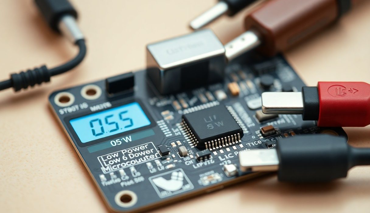
You will need a selection of instruments that match the current magnitude and temporal behavior of the device under test: a high-resolution DMM for DC checks, a power analyzer or USB power profiler (examples: Monsoon Power Monitor, Otii Arc, Keysight N6705C) for logged energy and long-term tests, and an oscilloscope with a current probe for transient capture. For low-power IoT work expect to measure currents from single-digit microamps to hundreds of milliamps, so choose tools that offer resolution down to 1 µA and sample rates of at least 100 kS/s for event tracing.
Include a precision shunt resistor sized so its drop is measurable without significantly loading the circuit; typical choices range from 0.01 Ω to 1 Ω depending on current span, and you should calculate power dissipation using P=I²R to ensure the shunt won’t overheat. In addition, use differential probes or isolation amplifiers to avoid ground loops, and consider an INA/ADC front-end (for example, INA219 or ADS1115) when you need a compact, integrated solution for ongoing product testing.
Testing Procedures
Start by defining a representative use-case cycle and calibrating your instruments against a known reference; then wire the shunt or current probe in series with the supply and measure both the supply voltage and the shunt voltage simultaneously so you can compute current and instantaneous power. Use the oscilloscope for capturing fast transients-set the sample rate to at least 10× the expected transient frequency-and use a power analyzer or data logger for long-duration energy measurements. For example, if a sensor wakes for 100 ms at 30 mA every 1 s and sleeps at 5 µA otherwise, capture several cycles to get statistical confidence.
Next, compute average current and energy from the logged waveform: integrate P(t)=V(t)·I(t) over the measurement interval T to get energy E and then Pavg = E/T. Using the example above, your average current = 0.1×30 mA + 0.9×5 µA ≈ 3.0045 mA, and at 3.3 V that corresponds to about 9.91 mW average power. Always report the measurement uncertainty, sampling rate, and any filtering applied so your results are reproducible.
When performing tests near mains or with high currents, isolate circuits and be aware that shunt resistors can dissipate significant heat-check that the shunt’s power rating exceeds the expected P=I²R and use proper fusing; improper wiring or overloads can be dangerous. For low-current, long-duration battery tests, reduce sampling to conserve data storage but trigger high-speed captures on events to avoid missing spikes; additionally, control ambient temperature because battery capacity and device leakage currents can shift by several percent per 10 °C.
Pros and Cons of Low Power Consumption Solutions
| Pros | Cons |
|---|---|
| Significantly longer battery life – aggressive duty‑cycling and ultra‑low‑power MCU sleep modes can extend field life by 2-5× or more for sensors. | Reduced peak performance – you may need to throttle CPU/GPU clocks and radio throughput, lowering peak throughput and latency. |
| Lower heat dissipation and improved reliability – less thermal stress reduces cooling needs and component aging. | Increased design complexity – DVFS, power gating and state machines add firmware/hardware complexity and development time. |
| Smaller batteries and power supplies – BOM and enclosure size shrink, cutting system cost for many portable devices. | Longer wake/sleep transition times – wake-ups can be from microseconds to milliseconds or even tens of milliseconds, impacting real‑time tasks. |
| Enables always‑on and IoT deployments – technologies like Bluetooth Low Energy can cut radio energy by up to ~90% versus classic Bluetooth. | Standby leakage and process variability – at advanced nodes leakage can dominate, causing unpredictable standby currents across temperature/process. |
| Opportunities for energy harvesting and maintenance‑free devices – solar or vibration harvesting becomes practical for low‑duty sensors. | Testing and verification burden – validating all power states, transitions and corner cases increases QA cycles and test matrix size. |
| Regulatory and marketing advantages – lower energy use helps meet energy ratings and sustainability goals. | Higher NRE or specialized components – low‑power MCUs, PMICs and accurate RTCs can increase unit cost for low‑volume products. |
| Lower EMI and reduced cooling requirements – simplifies mechanical/thermal design in many systems. | Software complexity for reliability – you must manage state retention, context save/restore and watchdogs across power domains. |
| Scalability for large fleets – per‑node energy savings multiply in wide deployments, lowering total maintenance. | OTA/update challenges – remote updates consume bursts of energy and may require special power‑budget planning. |
Advantages of Low Power Electronics
You can materially extend device lifetime by combining hardware features (power gating, low‑leakage transistors) with firmware strategies (duty cycling, event‑driven wake-ups). For example, asset trackers that sleep 99% of the time and use Bluetooth Low Energy often achieve multi‑year operation on a CR2032 coin cell (≈220-240 mAh), because BLE and optimized duty cycles cut radio energy by roughly 90% compared with legacy radios.
Design techniques like DVFS (dynamic voltage and frequency scaling) give you a strong leverage point: dynamic power scales approximately with V²·f, so a modest voltage reduction can yield large savings during normal workloads. You also reduce thermal design constraints – servers using dynamic power capping frequently lower cooling and rack density costs, while edge devices avoid heat‑related failures, improving overall system reliability.
Disadvantages and Trade-offs
You will face trade‑offs in latency and peak capability: putting subsystems into deep sleep saves energy but introduces wake latencies that can range from microseconds for shallow states to milliseconds or more for deep retention modes – unacceptable in some real‑time or safety‑critical applications. Additionally, power gating and aggressive clock gating increase the chance of brownouts during transient current spikes unless you provision capacitors and PMIC headroom for bursts (plan for 100-500 mA peaks on radios or actuators).
Development overhead rises because you must verify every combination of power state, input condition and temperature corner. Leakage currents can become the dominant loss at sub‑20 nm nodes, so even with aggressive sleep you might see standby currents in the nanoamp to low‑microamp range per domain that add up across a complex SoC. That requires careful partitioning and sometimes extra silicon features, which increase BOM and NRE.
Testing and mitigation strategies are crucial: you should instrument prototypes with nano‑amp meters and power‑trace analyzers, model worst‑case wake frequency, and include hardware watchdogs and safe‑recovery paths to prevent corrupted flash during low‑voltage events. In practice, you often balance energy savings vs. latency, cost and verification effort – plan for firmware state machines that minimize wake time, allocate decoupling for peak currents, and set clear fallbacks for safety‑critical paths.
Future Trends in Low Power Consumption Technologies
You’ll see the next wave focused on co-design: hardware, firmware, and algorithms engineered together to squeeze energy out of every operation. For example, combining aggressive DVFS, power gating, and tiny neural networks lets edge devices perform local inference at sub-millijoule per inference in real deployments, reducing uplink energy and latency. At the system level, expect chiplet and 3D-stacked architectures to cut off-chip communication energy dramatically by bringing memory and accelerators closer to compute, while advanced packaging lowers parasitic losses that previously dominated mobile and IoT power budgets.
Manufacturing and materials will keep pushing boundaries too: moving beyond planar nodes and introducing GaN/SiC in power converters will shrink losses in power delivery, and energy-proportional OSs and compilers will make your applications idle more efficiently. In parallel, energy harvesting (thermal, vibration, RF) now routinely supplies microwatts to milliwatts in fielded sensors, enabling maintenance-free nodes; at the same time, near-threshold operation promises up to an order of magnitude reduction in energy per operation but requires error-tolerant stacks and careful design trade-offs.
Emerging Innovations
Specialized accelerators and always-on microcontrollers are becoming standard: Google’s Edge TPU and similar NPUs deliver very high efficiency (on the order of several TOPS per watt in silicon optimized for inference), letting you run complex models locally rather than sending data to the cloud. Non-volatile memories such as MRAM and ReRAM are also moving into designs to eliminate standby leakage and shorten wake-up times, which is especially valuable for devices that sleep most of the time.
Architectural techniques like approximate computing, near-threshold voltage operation, and fine-grained body-bias control let you trade accuracy for energy when your workload allows it; for instance, near-threshold designs can reduce energy per operation by up to 10x in research and select products, but they increase soft-error rates and timing variability, so you’ll need robust error correction or adaptive tuning. Complementing these are advances in power-management ICs that integrate monitoring, dynamic control loops, and multi-source energy harvesting interfaces to maximize the usable energy from ambient sources in real-world conditions.
Market Demand and Applications
Automotive, wearables, industrial IoT, and edge AI are the primary drivers you should be watching: electric vehicles demand high-efficiency power electronics to extend range, while industrial sensors require multi-year battery life-LoRaWAN nodes routinely hit 10+ years on a single AA in field deployments. Data centers also push low-power innovation because energy is a major cost center; data centers account for roughly 1% of global electricity use, so any efficiency gain scales to substantial operational savings and emissions reductions.
Healthcare implants and remote monitoring create stringent requirements for ultra-low leakage and predictable lifetime: pacemakers and implantables force designers to prioritize reliability over peak performance, and you’ll see specialized low-power design flows and qualification regimes emerge for these markets. Regulations and procurement standards in the EU and California are accelerating uptake by setting minimum efficiency targets for consumer and industrial devices, which directly impacts your product roadmaps and supplier choices.
On the volume side, tens of billions of connected devices are driving economies of scale that reduce cost per watt for efficient components; market forecasts projecting around 20-30 billion connected endpoints in the near term mean suppliers are investing in low-power IP, optimized Process Design Kits (PDKs), and ecosystem tools so you can source components that meet stricter lifetime and thermal envelopes while keeping BOM costs competitive.
Conclusion
Now you see that minimizing power consumption is a strategic advantage: it extends battery life, lowers thermal stress, reduces system costs, and helps you meet regulatory and sustainability targets while preserving performance. Applying power-aware architecture, dynamic management, and careful component selection lets you deliver reliable products for mobile, IoT, and edge markets.
As you adopt low-power design practices, you improve user satisfaction, lengthen product lifecycles, and gain a competitive edge; invest in measurement, profiling, and iterative optimization to maximize these benefits and keep your systems efficient over time.