Many designers use optical coupling to isolate control circuits from power rails so hazardous high-voltage transients cannot reach your equipment or you, reducing shock and equipment damage. By converting electrical signals to light and back, optical isolators give you galvanic isolation and improved noise immunity, provide predictable safety margins, and enable safer debugging, regulatory compliance, and reliable signal transfer across isolation barriers.
Understanding Optical Coupling
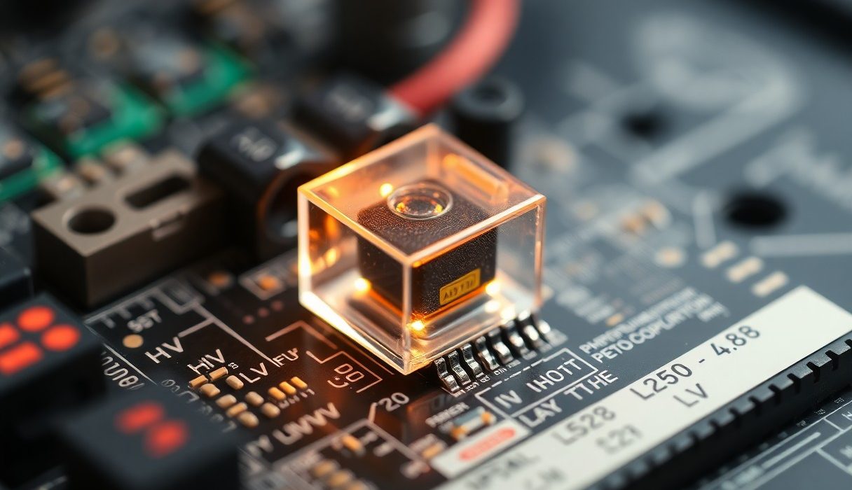
When you use an LED to drive a photosensor across an air gap, light becomes the only transfer mechanism and you get true galvanic isolation: the isolation barrier blocks DC and low-frequency leakage while the optical path transmits the control signal. Typical optocouplers are rated to withstand 3.75 kVrms (UL1577) for one minute; reinforced designs and solid-state relays can extend that to around 5 kVrms for applications that require higher working voltages. You should size the LED forward current and account for the device’s current transfer ratio so the output stage meets noise immunity and logic-level requirements.
Your choice also affects speed and long-term behavior: general-purpose phototransistor types trade speed for gain (response often in the 1 µs-3 ms range), whereas photodiode/receiver pairs or high-speed optocouplers can reach tens of nanoseconds to microseconds of propagation delay. In practice, industrial designs isolate a 24 V control plane from a 400 V mains using optocouplers rated for >3.75 kVrms and derate LED current to extend lifetime and reduce thermal stress.
| LED | Light source that defines input current and lifetime |
| Phototransistor | Gain stage for general-purpose isolation, higher CTR, slower |
| Photodiode + amplifier | High-speed, low-delay receivers for digital isolation |
| Phototriac | AC switch for mains control, used in triac driver circuits |
| Opto-MOSFET / SSR | Integrated solid-state switching with specified load current |
Types of Optical Coupling
You will commonly encounter several families: phototransistor optocouplers for simple level shifting and high gain, photodiode-based receivers for low propagation delay and digital isolation, phototriac devices where AC zero-cross switching is needed, and integrated solid-state relays or opto-MOSFETs when you need defined load currents up to a few amperes. For example, a phototransistor device with a CTR of 20-100% is handy for 5 V logic interfaces, while a photodiode pair might give you propagation delays under 200 ns for SPI isolation.
- Phototransistor – general-purpose, CTR typically 20-100%, response ~1 µs-3 ms.
- Photodiode / Receiver – low propagation delay (tens of ns-µs), used in USB or high-speed UART isolation.
- Phototriac – designed for AC mains switching, often rated for 1-2 A with built-in zero-cross options.
- Solid-state relay (SSR) – integrated devices that package LED + output switch, with load ratings from hundreds of mA to several A.
Assume that you match device family to the system requirement: choose photodiode-based isolators for high-speed serial lines and phototransistor types where simple level translation and noise rejection are more important than nanosecond speed.
Factors Influencing Performance
Key parameters you must manage include current transfer ratio (CTR), isolation voltage, propagation delay, and common-mode transient immunity (CMTI). CTR is expressed as a percentage of output current to input LED current and typically falls with higher temperatures and LED aging; expect CTR shifts of tens of percent over wide temperature ranges. CMTI is often specified in kV/µs for modern isolators-many industrial parts provide ratings in the low double-digit kV/µs range-so you should verify this when you design for fast switching in noisy environments.
- CTR – determines how much input current you need to achieve a given output, influenced by temperature and aging.
- Propagation delay – varies from tens of ns (high-speed receivers) to milliseconds (general-purpose phototransistors).
- Isolation voltage & creepage/clearance – specify per your safety standard (UL/IEC) and derate for pollution degree and altitude.
- CMTI – assessed in kV/µs; pick devices with margin above your worst-case dv/dt.
Perceiving how each parameter interacts lets you trade speed, noise immunity, and lifetime to meet system-level safety and functional goals.
More granular effects you need to evaluate are LED junction temperature, board-level creepage/clearance, contamination risks, and how packaging affects partial discharge and humidity sensitivity; for instance, a device that meets 3.75 kVrms in a clean lab may require larger creepage distances or conformal coating in a dusty, humid cabinet. Practical designs also derate LED drive by 20-30% where long MTBF is required, and you should test representative samples for CTR after 1,000-5,000 hours at elevated temperature if your product must operate for years in the field.
- LED junction temperature – higher temperature reduces light output and accelerates aging.
- Creepage & clearance – increase distances for higher pollution degrees or altitude.
- Aging & test margins – perform life tests (1,000-5,000 h) to track CTR drift and plan derating.
Perceiving these dependencies helps you set design margins that keep the isolation barrier reliable over the product lifetime.
Benefits of Optical Coupling
By inserting an optical barrier between circuits, you get galvanic isolation that blocks DC and low-frequency leakage currents, which directly reduces ground-loop noise and the risk of common-mode transients corrupting sensitive ADCs or communication lines. In practice that means you can separate high-voltage sections (for example, mains or inverter bridges) from low-voltage control logic without shunts or complex isolation transformers; many optocouplers are specified for isolation voltages in the 1.5 kV to 5 kV RMS range and can meet safety clearances required by industrial and some medical classes.
Signal-level benefits are tangible too: when you use optical coupling for gate drivers or serial links, you typically cut conducted EMI paths and improve noise immunity, letting you achieve cleaner switching edges and more reliable telemetry in harsh environments such as motor drives or PV inverters. High-speed LED/photodiode optocouplers and modern optical isolators support data rates from ~1 Mbps for legacy parts up to >10 Mbps for high-speed versions, so you can choose a device that balances isolation with throughput for your system.
Pros of Enhanced Electrical Isolation
You lower user and equipment risk by enforcing physical separation: isolation prevents hazardous voltages from appearing on user-accessible circuits, which simplifies compliance with standards like IEC/EN for basic and reinforced insulation. For instance, isolating a mains-sensing circuit with a 3-5 kV-rated optocoupler helped a commercial UPS design reduce leakage current to under regulatory limits while avoiding bulky transformers, shaving both weight and BOM cost.
You also improve system reliability under noisy conditions. Optical isolation eliminates direct conductive paths for ground-loop currents that otherwise induce offset errors on precision measurements; engineers working on three-phase energy meters have documented reductions in measurement error by several percent after adding optocouplers to the sensing path. And because the optical channel is immune to DC offsets, you can interface floating supplies or battery stacks without complex common-reference schemes.
Cons and Limitations
Optical coupling is not a free lunch: you trade some bandwidth and latency for isolation. General-purpose optocouplers often exhibit propagation delays in the microsecond range (typical 3-10 µs) and jitter that can complicate tight control loops, whereas high-speed variants reduce delay to the tens to hundreds of nanoseconds at higher cost. You must also account for LED aging and temperature dependence-photodiode current transfer ratio (CTR) can decline over time and at high temperatures, which may require derating or periodic calibration in long-life products.
Physical constraints matter as well: to achieve the stated isolation voltage you still need proper PCB creepage and clearance distances, which increases board area and enclosures size in high-voltage designs. Power consumption and drive requirements are another limitation-many optocouplers require a modest LED drive current (often 1-20 mA), so battery-operated systems may prefer alternatives, and bidirectional signaling can become complex without additional circuitry.
Failure modes are notable: partial degradation of the LED or detector usually manifests as reduced CTR and increased propagation delay, not a clean open-circuit, which can cause intermittent logic errors that are hard to diagnose. In safety-critical designs you should assume degradation over tens of thousands of hours and design diagnostics or redundancy accordingly, and verify that the selected optocoupler meets the required insulation lifetime and temperature derating per the application’s safety standard.
Tips for Effective Implementation
Component selection and ratings
Select an optocoupler with an isolation voltage margin above your system’s maximum transient: many signal optocouplers are specified for ~3.75 kVrms (1 minute) while reinforced-insulation parts target 5 kV or more for medical/industrial apps. Check the device CTR range (typical 20-300%) and the propagation delay (from ~100 ns for high-speed types to several µs for general-purpose units) so you can size LED drive current (often 1-20 mA) and any pull-ups/pull-downs to meet timing at your data rate. Treat insufficient voltage rating and marginal creepage as dangerous failure modes: breakdown, arcing, or latent insulation degradation will create safety hazards and intermittent faults under surge or humidity stress.
- Verify manufacturer isolation voltage test conditions and backing standards (UL1577, IEC 60747-5-5).
- Match CMTI (common‑mode transient immunity) to your environment; aim for ≥10 kV/µs for industrial drives, higher for fast switching.
- Confirm CTR at the operating temperature and LED current, and de-rate for lifetime/temperature.
- Plan mechanical spacing: enforce PCB creepage and clearance per target standards (use 8 mm as a practical starting point for 3.75-5 kVrms designs when no stricter spec exists).
- Use conformal coating or potting when contamination or humidity could reduce surface resistance.
PCB layout, testing, and certification
Place the isolator on the board so that the electrical isolation barrier follows the shortest internal leakage path but maximizes external creepage and clearance-route high-voltage traces away from low-voltage sections and avoid vias in the isolation gap unless fitted with insulating collars or resin. Add local decoupling on both sides of the barrier (10-100 nF near supplies) and implement single‑point grounding or controlled star returns to reduce ground-loop currents; in one industrial CAN node example, selecting an optocoupler with >50 kV/µs CMTI and relocating bypass caps to the isolation boundaries eliminated >90% of EMI-induced packet errors at 1 Mbps. Perform an AC dielectric (hipot) test at the device-rated voltage for 60 seconds and run partial discharge checks if your design must meet IEC 60601-1 medical insulation requirements; pursue UL1577 or IEC approvals early to avoid rework during certification. Knowing the precise part ratings, layout distances, and test procedures lets you validate safety margins and prevent costly field failures.
Step-by-Step Guide to Optical Coupling
Prepare and select components
Begin by defining your isolation and speed targets: for mains-side designs you should plan for at least 3-5 kV isolation and a safety margin above your system’s peak voltage, while for control signals note that general-purpose optocouplers typically have propagation delays of 2-10 µs and CTRs in the 20-200% range. Use a specific example: if you need to isolate a 115 VAC line-to-low-voltage microcontroller interface, pick an optocoupler with a 5 kV isolation rating, LED forward current spec that meets your driver (e.g., 1-5 mA for low-power logic), and a datasheet propagation delay that supports your baud rate (for UART at 115200 baud a ≤10 µs delay is acceptable; for SPI at >1 MHz choose a high-speed device with <1 µs).
Integrate, layout, and test
When you place the device, size the input resistor to achieve the required LED current (use Ohm’s law: (Vin−Vf)/R) and verify CTR under the expected temperature; practical designs often target 1-5 mA LED drive to balance lifetime and switching performance. After routing, enforce adequate creepage/clearance-typically 4-8 mm depending on pollution degree and working voltage-and perform insulation verification per the optocoupler datasheet, including a hipot/insulation-withstand test commonly in the 3-5 kV range for system validation; log leakage and switching tests (rise/fall, propagation delay, and jitter) so you can compare against the component’s rated values and catch any assembly or layout issues early.
Quick Implementation Steps
| Step | Action / Detail |
| 1. Define specs | Set isolation voltage (e.g., 3-5 kV), required data rate, and environmental limits. |
| 2. Select part | Match CTR, propagation delay (≤10 µs general, <1 µs for high-speed), and isolation rating. |
| 3. Design input | Calculate series resistor for LED drive (target 1-5 mA for low-power logic). |
| 4. PCB layout | Maintain creepage/clearance (4-8 mm as required), keep noisy traces away from photodiode/receiver. |
| 5. Test | Perform functional, leakage, and insulation-withstand (hipot) tests per datasheet; record timings and leakage currents. |
Applications of Optical Coupling in Industry
Power conversion and motor control
You deploy optical coupling extensively in IGBT and MOSFET gate drivers, where isolators rated between 2.5 kV and 5 kV RMS (many commercial parts specify 3.75 kVrms for 1 minute) separate low-voltage control electronics from 600-1,200 V DC bus rails in industrial inverters and traction drives. In practice, this lets you place microcontrollers and sensors on a common low-voltage ground while the power stage runs at high potential, eliminating ground loops and reducing EMI coupling into control logic. Specialized digital optical isolators also provide very high common-mode transient immunity (CMTI), often exceeding 50 kV/µs, which prevents false switching during fast voltage transients in applications like grid-tied PV inverters and servo systems.
Medical, measurement, and safety systems
You rely on optical isolation to meet safety standards and preserve measurement integrity: patient-connected medical devices and many test instruments require reinforced or double isolation, and optical couplers with specified isolation voltages and certified creepage/clearance help you achieve that. For example, isolated data-acquisition modules and oscilloscope front-ends commonly use optocouplers or optical isolators rated for several kilovolts to prevent dangerous leakage currents; a single-point isolation failure can be life-threatening, so you should select components with appropriate IEC/UL certifications and validated dielectric withstand levels. In factory automation and hazardous-area instrumentation, replacing bulky transformers with optical isolators often reduces size and cost while maintaining multi-kilovolt isolation and improving signal bandwidth for fast sensing and control loops.
Future Trends in Optical Coupling
Higher speeds and tighter integration
Advances in silicon photonics and VCSEL arrays are pushing optical coupling from Mbps into tens of gigabits per second; you can now find optical isolators and integrated photonic transceivers delivering 10-25 Gbps per channel in data‑center links and high-speed industrial networks. As manufacturers put photonic waveguides and modulators directly on CMOS, your designs will shrink board area by more than 50% while lowering parasitics that used to limit rise times-this directly improves isolation performance at high data rates. Standards and test methods are evolving too (for example, suppliers reference IEC 60747‑5‑5 and related safety tests), so you should plan for component choices that meet both high-throughput and regulatory requirements.
Power electronics and safety‑critical adoption
You’re already seeing optical coupling migrate into isolated gate drivers and telemetry for SiC and GaN power stages rated 650-1200 V, where kilovolt‑level isolation and fast switching are both required; field studies show optically isolated drivers reduce common‑mode disturbances and enable tighter timing control compared with transformer‑based isolation. In safety‑critical sectors-medical, transportation, and industrial automation-manufacturers increasingly pair optical isolation with built‑in diagnostics and redundancy so your system can prevent dangerous ground currents and meet double/reinforced insulation requirements (examples include medical devices complying with IEC 60601 and industrial converters with reinforced isolation barriers). Expect more integrated optical modules that combine isolation, monitoring, and fail‑safe logic to simplify certification and reduce your validation effort.
Conclusion
So you gain reliable galvanic isolation when you use optical coupling, which prevents hazardous current transfer between domains, reduces ground-loop and common‑mode noise, and shields your low-voltage electronics from high-voltage transients. You can preserve signal integrity across large potential differences and meet safety and regulatory insulation ratings by selecting appropriate optocouplers or fiber links that provide specified isolation voltages and EMI immunity.
So when you design with optical coupling, evaluate bandwidth, propagation delay, linearity, and transfer characteristics to match your control and sensing needs, and account for creepage/clearance and surge protection to maximize long-term performance. By choosing the right optical isolation approach, you simplify system grounding, improve safety margins, and maintain accurate, low-noise communication between isolated domains.